
Datasheet


MSP430FR573x
MSP430FR572x
www.ti.com
SLAS639H –JULY 2011–REVISED SEPTEMBER 2013
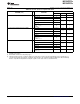
Table 42. Port P1 (P1.0 to P1.2) Pin Functions
CONTROL BITS/SIGNALS
PIN NAME (P1.x) x FUNCTION
P1DIR.x P1SEL1.x P1SEL0.x
P1.0/TA0.1/DMAE0/RTCCLK/A0/CD0/VeREF- 0 P1.0 (I/O) I: 0; O: 1 0 0
TA0.CCI1A 0
0 1
TA0.1 1
DMAE0 0
1 0
RTCCLK 1
A0
(1) (2)
CD0
(1) (3)
X 1 1
VeREF-
(1) (2)
P1.1/TA0.2/TA1CLK/CDOUT/A1/CD1/VeREF+ 1 P1.1 (I/O) I: 0; O: 1 0 0
TA0.CCI2A 0
0 1
TA0.2 1
TA1CLK 0
1 0
CDOUT 1
A1
(1) (2)
CD1
(1) (3)
X 1 1
VeREF+
(1) (2)
P1.2/TA1.1/TA0CLK/CDOUT/A2/CD2 2 P1.2 (I/O) I: 0; O: 1 0 0
TA1.CCI1A 0
0 1
TA1.1 1
TA0CLK 0
1 0
CDOUT 1
A2
(1) (2)
X 1 1
CD2
(1) (3)
(1) Setting P1SEL1.x and P1SEL0.x disables the output driver as well as the input Schmitt trigger to prevent parasitic cross currents when
applying analog signals.
(2) Not available on all devices and package types.
(3) Setting the CDPD.x bit of the comparator disables the output driver as well as the input Schmitt trigger to prevent parasitic cross
currents when applying analog signals. Selecting the CDx input pin to the comparator multiplexer with the CDx bits automatically
disables output driver and input buffer for that pin, regardless of the state of the associated CDPD.x bit.
Copyright © 2011–2013, Texas Instruments Incorporated Submit Documentation Feedback 71