
Datasheet


MSP430FR573x
MSP430FR572x
SLAS639H –JULY 2011–REVISED SEPTEMBER 2013
www.ti.com
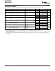
Comparator_D
over operating free-air temperature range (unless otherwise noted)
PARAMETER TEST CONDITIONS MIN TYP MAX UNIT
Overdrive = 10 mV,
50 100 200 ns
VIN- = (VIN+ – 400 mV) to (VIN+ + 10 mV)
Propagation delay, Overdrive = 100 mV,
t
pd
80 ns
AVCC = 2 V to 3.6 V VIN- = (VIN+ – 400 mV) to (VIN+ + 100 mV)
Overdrive = 250 mV,
50 ns
(VIN+ – 400 mV) to (VIN+ + 250 mV)
CDF = 1, CDFDLY = 00 0.3 0.5 0.9 µs
Filter timer added to the
CDF = 1, CDFDLY = 01 0.5 0.9 1.5 µs
t
filter
propagation delay of the
CDF = 1, CDFDLY = 10 0.9 1.6 2.8 µs
comparator
CDF = 1, CDFDLY = 11 1.6 3.0 5.5 µs
V
offset
Input offset AVCC = 2 V to 3.6 V -20 20 mV
Common mode input
V
ic
AVCC = 2 V to 3.6 V 0 AVCC - 1 V
range
I
comp(AVCC)
Comparator only CDON = 1, AVCC = 2 V to 3.6 V 29 34 µA
Reference buffer and R-
I
ref(AVCC)
CDREFLx = 01, AVCC = 2 V to 3.6 V 20 24 µA
ladder
CDON = 0 to CDON = 1,
t
enable,comp
Comparator enable time 1.1 2.0 µs
AVCC = 2 V to 3.6 V
Resistor ladder enable CDON = 0 to CDON = 1,
t
enable,rladder
1.1 2.0 µs
time AVCC = 2 V to 3.6 V
VIN × VIN × VIN ×
Reference voltage for a VIN = voltage input to the R-ladder,
V
CB_REF
(n + 0.5) (n + 1) (n + 1.5) V
tap n = 0 to 31
/ 32 / 32 / 32
FRAM
over recommended ranges of supply voltage and operating free-air temperature (unless otherwise noted)
PARAMETER TEST CONDITIONS MIN TYP MAX UNIT
DV
CC(WRITE)
Write supply voltage 2.0 3.6 V
t
WRITE
Word or byte write time 120 ns
t
ACCESS
Read access time
(1)
60 ns
t
PRECHARGE
Precharge time
(1)
60 ns
t
CYCLE
Cycle time, read or write operation
(1)
120 ns
Read and write endurance 10
15
cycles
T
J
= 25°C 100
t
Retention
Data retention duration T
J
= 70°C 40 years
T
J
= 85°C 10
(1) When using manual wait state control, see the MSP430FR57xx Family User's Guide (SLAU272) for recommended settings for common
system frequencies.
68 Submit Documentation Feedback Copyright © 2011–2013, Texas Instruments Incorporated