
Datasheet


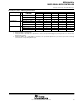


Table Of Contents
- features
- description
- AVAILABLE OPTIONS
- DEVELOPMENT TOOL SUPPORT
- pin designation, MSP430xG461xIPZ
- pin designation, MSP430xG461xIZQW (top view)
- functional block diagram
- Terminal Functions
- short-form description
- CPU
- instruction set
- operating modes
- interrupt vector addresses
- special function registers (SFRs)
- memory organization
- bootstrap loader (BSL)
- flash memory
- peripherals
- DMA controller
- oscillator and system clock
- brownout, supply voltage supervisor
- brownout, supply voltage supervisor
- digital I/O
- Basic Timer1 and Real-Time Clock
- LCD_A drive with regulated charge pump
- watchdog timer (WDT+)
- universal serial communication interface (USCI)
- USART1
- hardware multiplier
- Timer_A3
- Timer_B7
- Comparator_A
- ADC12
- DAC12
- OA
- peripheral file map
- absolute maximum ratings over operating free-air temperature
- recommended operating conditions
- electrical characteristics
- supply current into AVCC + DVCC excluding external current
- supply current into AVCC + DVCC excluding external current
- Schmitt-trigger inputs -- Ports P1 to P10, RST/NMI, JTAG (TCK, TMS, TDI/TCLK, TDO/TDI)
- inputs Px.x, TAx, TBx
- leakage current -- Ports P1 to P10
- outputs -- Ports P1 to P10
- output frequency
- wake-up LPM3
- RAM
- LCD_A
- Comparator_A
- POR/brownout reset (BOR)
- SVS (supply voltage supervisor/monitor)
- DCO
- crystal oscillator, LFXT1 oscillator
- crystal oscillator, LFXT1 oscillator
- crystal oscillator, XT2 oscillator
- USCI (UART mode)
- USCI (SPI master mode)
- USCI (SPI slave mode)
- USCI (I2C mode)
- USART1
- 12-bit ADC, power supply and input range conditions
- 12-bit ADC, power supply and input range conditions
- 12-bit ADC, external reference
- 12-bit ADC, built-in reference
- 12-bit ADC, timing parameters
- 12-bit ADC, linearity parameters
- 12-bit ADC, temperature sensor and built-in VMID
- 12-bit DAC, supply specifications
- 12-bit DAC, linearity specifications
- 12-bit DAC, output specifications
- 12-bit DAC, reference input specifications
- 12-bit DAC, dynamic specifications; Vref = VCC, DAC12IR = 1
- operational amplifier OA, supply specifications
- operational amplifier OA, input/output specifications
- operational amplifier OA, dynamic specifications
- operational amplifier OA feedback network, noninverting amplifier mode (OAFCx = 4)
- operational amplifier OA feedback network, inverting amplifier mode (OAFCx = 6)
- flash memory (MSP430FG461x devices only)
- JTAG interface
- JTAG fuse
- APPLICATION INFORMATION
- input/output schematics
- Port P1, P1.0 to P1.5, input/output with Schmitt trigger
- Port P1 (P1.0 to P1.5) pin functions
- Port P1, P1.6, P1.7, input/output with Schmitt trigger
- Port P1 (P1.6 and P1.7) pin functions
- port P2, P2.0 to P2.3, P2.6 to P2.7, input/output with Schmitt trigger
- Port P2 (P2.0, P2.1, P2.2, P2.3, P2.6 and P2.7) pin functions
- port P2, P2.4 to P2.5, input/output with Schmitt trigger
- Port P2 (P2.4 and P2.5) pin functions
- port P3, P3.0 to P3.3, input/output with Schmitt trigger
- Port P3 (P3.0 to P3.3) pin functions
- port P3, P3.4 to P3.7, input/output with Schmitt trigger
- Port P3 (P3.4 to P3.7) pin functions
- port P4, P4.0 to P4.1, input/output with Schmitt trigger
- Port P4 (P4.0 to P4.1) pin functions
- port P4, P4.2 to P4.7, input/output with Schmitt trigger
- Port P4 (P4.2 to P4.5) pin functions
- port P5, P5.0, input/output with Schmitt trigger
- Port P5 (P5.0) pin functions
- port P5, P5.1, input/output with Schmitt trigger
- Port P5 (P5.1) pin functions
- port P5, P5.2 to P5.4, input/output with Schmitt trigger
- Port P5 (P5.2 to P5.4) pin functions
- port P5, P5.5 to P5.7, input/output with Schmitt trigger
- Port P5 (P5.5 to P5.7) pin functions
- port P6, P6.0, P6.2, and P6.4, input/output with Schmitt trigger
- Port P6 (P6.0, P6.2, and P6.4) pin functions
- port P6, P6.1, P6.3, and P6.5 input/output with Schmitt trigger
- Port P6 (P6.1, P6.3, and P6.5) pin functions
- port P6, P6.6, input/output with Schmitt trigger
- Port P6 (P6.6) pin functions
- port P6, P6.7, input/output with Schmitt trigger
- Port P6 (P6.7) pin functions
- port P7, P7.0 to P7.3, input/output with Schmitt trigger
- Port P7 (P7.0 to P7.1) pin functions
- port P7, P7.4 to P7.7, input/output with Schmitt trigger
- Port P7 (P7.4 to P7.5) pin functions
- port P8, P8.0 to P8.7, input/output with Schmitt trigger
- Port P8 (P8.0 to P8.1) pin functions
- Port P8 (P8.6 to P8.7) pin functions
- port P9, P9.0 to P9.7, input/output with Schmitt trigger
- Port P9 (P9.0 to P9.1) pin functions
- port P10, P10.0 to P10.5, input/output with Schmitt trigger
- Port P10 (P10.0 to P10.1) pin functions
- port P10, P10.6, input/output with Schmitt trigger
- Port P10 (P10.6) pin functions
- port P10, P10.7, input/output with Schmitt trigger
- Port P10 (P10.7) pin functions
- VeREF+/DAC0
- JTAG pins TMS, TCK, TDI/TCLK, TDO/TDI, input/output with Schmitt trigger or output
- JTAG fuse check mode
- input/output schematics
- Data Sheet Revision History

MSP430xG461x
MIXED SIGNAL MICROCONTROLLER
SLAS508I − APRIL 2006 − REVISED MARCH 2011
89
POST OFFICE BOX 655303 • DALLAS, TEXAS 75265
Port P7 (P7.0 to P7.1) pin functions
PIN NAME (P7 X)
X
FUNCTION
CONTROL BITS / SIGNALS
PIN NAME (P7.X)
X FUNCTION
P7DIR.x P7SEL.x LCDS32
P7.0/UCA0STE/S33 0
P7.0 (I/O) I: 0; O: 1 0 0
USCI_A0.UCA0STE (see Notes 1, 2) X 1 0
S33 (see Note 1) X X 1
P7.1/UCA0SIMO/S32 1
P7.1 (I/O) I: 0; O: 1 0 0
USCI_A0.UCA0SIMO (see Notes 1, 2) X 1 0
S32 (see Note 1) X X 1
P7.2/UCA0SOMI/S31 2
P7.2 (I/O) I: 0; O: 1 0 0
USCI_A0.UCA0SOMI (see Notes 1, 3) X 1 0
S31 (see Note 1) X X 1
P7.3/UCA0CLK/S30 3
P7.3 (I/O) I: 0; O: 1 0 0
USCI_A0.UCA0CLK (see Notes 1, 3) X 1 0
S30 (see Note 1) X X 1
NOTES: 1. X: Don’t care
2. The pin direction is controlled by the USCI module.
3. The pin direction is controlled by the USCI module.