
Datasheet


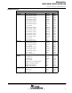


Table Of Contents
- features
- description
- AVAILABLE OPTIONS
- DEVELOPMENT TOOL SUPPORT
- pin designation, MSP430xG461xIPZ
- pin designation, MSP430xG461xIZQW (top view)
- functional block diagram
- Terminal Functions
- short-form description
- CPU
- instruction set
- operating modes
- interrupt vector addresses
- special function registers (SFRs)
- memory organization
- bootstrap loader (BSL)
- flash memory
- peripherals
- DMA controller
- oscillator and system clock
- brownout, supply voltage supervisor
- brownout, supply voltage supervisor
- digital I/O
- Basic Timer1 and Real-Time Clock
- LCD_A drive with regulated charge pump
- watchdog timer (WDT+)
- universal serial communication interface (USCI)
- USART1
- hardware multiplier
- Timer_A3
- Timer_B7
- Comparator_A
- ADC12
- DAC12
- OA
- peripheral file map
- absolute maximum ratings over operating free-air temperature
- recommended operating conditions
- electrical characteristics
- supply current into AVCC + DVCC excluding external current
- supply current into AVCC + DVCC excluding external current
- Schmitt-trigger inputs -- Ports P1 to P10, RST/NMI, JTAG (TCK, TMS, TDI/TCLK, TDO/TDI)
- inputs Px.x, TAx, TBx
- leakage current -- Ports P1 to P10
- outputs -- Ports P1 to P10
- output frequency
- wake-up LPM3
- RAM
- LCD_A
- Comparator_A
- POR/brownout reset (BOR)
- SVS (supply voltage supervisor/monitor)
- DCO
- crystal oscillator, LFXT1 oscillator
- crystal oscillator, LFXT1 oscillator
- crystal oscillator, XT2 oscillator
- USCI (UART mode)
- USCI (SPI master mode)
- USCI (SPI slave mode)
- USCI (I2C mode)
- USART1
- 12-bit ADC, power supply and input range conditions
- 12-bit ADC, power supply and input range conditions
- 12-bit ADC, external reference
- 12-bit ADC, built-in reference
- 12-bit ADC, timing parameters
- 12-bit ADC, linearity parameters
- 12-bit ADC, temperature sensor and built-in VMID
- 12-bit DAC, supply specifications
- 12-bit DAC, linearity specifications
- 12-bit DAC, output specifications
- 12-bit DAC, reference input specifications
- 12-bit DAC, dynamic specifications; Vref = VCC, DAC12IR = 1
- operational amplifier OA, supply specifications
- operational amplifier OA, input/output specifications
- operational amplifier OA, dynamic specifications
- operational amplifier OA feedback network, noninverting amplifier mode (OAFCx = 4)
- operational amplifier OA feedback network, inverting amplifier mode (OAFCx = 6)
- flash memory (MSP430FG461x devices only)
- JTAG interface
- JTAG fuse
- APPLICATION INFORMATION
- input/output schematics
- Port P1, P1.0 to P1.5, input/output with Schmitt trigger
- Port P1 (P1.0 to P1.5) pin functions
- Port P1, P1.6, P1.7, input/output with Schmitt trigger
- Port P1 (P1.6 and P1.7) pin functions
- port P2, P2.0 to P2.3, P2.6 to P2.7, input/output with Schmitt trigger
- Port P2 (P2.0, P2.1, P2.2, P2.3, P2.6 and P2.7) pin functions
- port P2, P2.4 to P2.5, input/output with Schmitt trigger
- Port P2 (P2.4 and P2.5) pin functions
- port P3, P3.0 to P3.3, input/output with Schmitt trigger
- Port P3 (P3.0 to P3.3) pin functions
- port P3, P3.4 to P3.7, input/output with Schmitt trigger
- Port P3 (P3.4 to P3.7) pin functions
- port P4, P4.0 to P4.1, input/output with Schmitt trigger
- Port P4 (P4.0 to P4.1) pin functions
- port P4, P4.2 to P4.7, input/output with Schmitt trigger
- Port P4 (P4.2 to P4.5) pin functions
- port P5, P5.0, input/output with Schmitt trigger
- Port P5 (P5.0) pin functions
- port P5, P5.1, input/output with Schmitt trigger
- Port P5 (P5.1) pin functions
- port P5, P5.2 to P5.4, input/output with Schmitt trigger
- Port P5 (P5.2 to P5.4) pin functions
- port P5, P5.5 to P5.7, input/output with Schmitt trigger
- Port P5 (P5.5 to P5.7) pin functions
- port P6, P6.0, P6.2, and P6.4, input/output with Schmitt trigger
- Port P6 (P6.0, P6.2, and P6.4) pin functions
- port P6, P6.1, P6.3, and P6.5 input/output with Schmitt trigger
- Port P6 (P6.1, P6.3, and P6.5) pin functions
- port P6, P6.6, input/output with Schmitt trigger
- Port P6 (P6.6) pin functions
- port P6, P6.7, input/output with Schmitt trigger
- Port P6 (P6.7) pin functions
- port P7, P7.0 to P7.3, input/output with Schmitt trigger
- Port P7 (P7.0 to P7.1) pin functions
- port P7, P7.4 to P7.7, input/output with Schmitt trigger
- Port P7 (P7.4 to P7.5) pin functions
- port P8, P8.0 to P8.7, input/output with Schmitt trigger
- Port P8 (P8.0 to P8.1) pin functions
- Port P8 (P8.6 to P8.7) pin functions
- port P9, P9.0 to P9.7, input/output with Schmitt trigger
- Port P9 (P9.0 to P9.1) pin functions
- port P10, P10.0 to P10.5, input/output with Schmitt trigger
- Port P10 (P10.0 to P10.1) pin functions
- port P10, P10.6, input/output with Schmitt trigger
- Port P10 (P10.6) pin functions
- port P10, P10.7, input/output with Schmitt trigger
- Port P10 (P10.7) pin functions
- VeREF+/DAC0
- JTAG pins TMS, TCK, TDI/TCLK, TDO/TDI, input/output with Schmitt trigger or output
- JTAG fuse check mode
- input/output schematics
- Data Sheet Revision History

MSP430xG461x
MIXED SIGNAL MICROCONTROLLER
SLAS508I − APRIL 2006 − REVISED MARCH 2011
27
POST OFFICE BOX 655303 • DALLAS, TEXAS 75265
peripheral file map (continued)
PERIPHERALS WITH BYTE ACCESS (CONTINUED)
USCI
USCI I2C Slave Address UCBI2CSA 011Ah
USCI I2C Own Address UCBI2COA 0118h
USCI Synchronous Transmit Buffer UCBTXBUF 06Fh
USCI Synchronous Receive Buffer UCBRXBUF 06Eh
USCI Synchronous Status UCBSTAT 06Dh
USCI I2C Interrupt Enable UCBI2CIE 06Ch
USCI Synchronous Bit Rate 1 UCBBR1 06Bh
USCI Synchronous Bit Rate 0 UCBBR0 06Ah
USCI Synchronous Control 1 UCBCTL1 069h
USCI Synchronous Control 0 UCBCTL0 068h
USCI Transmit Buffer UCATXBUF 067h
USCI Receive Buffer UCARXBUF 066h
USCI Status UCASTAT 065h
USCI Modulation Control UCAMCTL 064h
USCI Baud Rate 1 UCABR1 063h
USCI Baud Rate 0 UCABR0 062h
USCI Control 1 UCACTL1 061h
USCI Control 0 UCACTL0 060h
USCI IrDA Receive Control UCAIRRCTL 05Fh
USCI IrDA Transmit Control UCAIRTCTL 05Eh
USCI LIN Control UCAABCTL 05Dh
Comparator_A
Comparator_A port disable CAPD 05Bh
p
_
Comparator_A control 2 CACTL2 05Ah
Comparator_A control 1 CACTL1 059h
BrownOUT, SVS SVS control register (Reset by brownout signal) SVSCTL 056h
FLL+Clock
FLL+ Control 1 FLL_CTL1 054h
FLL+ Control 0 FLL_CTL0 053h
System clock frequency control SCFQCTL 052h
System clock frequency integrator SCFI1 051h
System clock frequency integrator SCFI0 050h
RTC (Basic Timer 1)
Real Time Clock Year High Byte RTCYEARH 04Fh
()
Real Time Clock Year Low Byte RTCYEARL 04Eh
Real Time Clock Month RTCMON 04Dh
Real Time Clock Day of Month RTCDAY 04Ch
Basic Timer1 Counter 2 BTCNT2 047h
Basic Timer1 Counter 1 BTCNT1 046h
Real Time Counter 4
(Real Time Clock Day of Week)
RTCNT4
(RTCDOW)
045h
Real Time Counter 3
(Real Time Clock Hour)
RTCNT3
(RTCHOUR)
044h
Real Time Counter 2
(Real Time Clock Minute)
RTCNT2
(RTCMIN)
043h
Real Time Counter 1
(Real Time Clock Second)
RTCNT1
(RTCSEC)
042h
Real Time Clock Control RTCCTL 041h
Basic Timer1 Control BTCTL 040h