
Datasheet
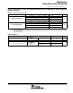


Table Of Contents
- features
- description
- Available Options
- pin designation, DL package
- pin designation, RGZ package
- functional block diagram
- Terminal Functions
- short-form description
- absolute maximum ratings
- recommended operating conditions
- electrical characteristics
- supply current into AVCC + DVCC excluding external current
- Schmitt-trigger inputs − Ports P1, P2, P5, and P6; RST/NMI; JTAG: TCK, TMS, TDI/TCLK, TDO/TDI
- inputs Px.x, TAx
- leakage current − Ports P1, P2, P5, and P6
- outputs − Ports P1, P2, P5, and P6
- output frequency
- wake-up LPM3
- RAM
- LCD_A
- POR/brownout reset (BOR)
- DCO
- crystal oscillator, LFXT1 oscillator
- SD16_A, power supply and recommended operating conditions
- SD16_A, input range
- SD16_A, performance
- SD16_A, temperature sensor
- SD16_A, built-in voltage reference
- SD16_A, reference output buffer
- SD16_A, external reference input
- 12-bit DAC, supply specifications
- 12-bit DAC, linearity specifications
- 12-bit DAC, output specifications
- 12-bit DAC, reference input specifications
- 12-bit DAC, dynamic specifications
- operational amplifier OA, supply specifications
- operational amplifier OA, input/output specifications
- operational amplifier OA, dynamic specifications
- switches to ground
- flash memory
- JTAG interface
- JTAG fuse
- input/output schematics
- Port P1 pin schematic: P1.0, P1.1, input/output with Schmitt−trigger
- Port P1 pin schematic: P1.2, input/output with Schmitt−trigger and analog functions
- Port P1 pin schematic: P1.3, P1.5, P1.7, input/output with Schmitt−trigger and analog functions
- Port P1 pin schematic: P1.4, input/output with Schmitt−trigger and analog functions
- Port P1 pin schematic: P1.6, input/output with Schmitt−trigger and analog functions
- Port P2 pin schematic: P2.0 to P2.1, input/output with Schmitt−trigger, LCD and analog functions
- Port P2 pin schematic: P2.2 to P2.7, input/output with Schmitt−trigger, LCD and analog functions
- Port P5 pin schematic: P5.0, P5.1, P5.5 to P5.7, input/output with Schmitt−trigger and LCDfunctions
- Port P5 pin schematic: P5.2 to P5.4, input/output with Schmitt−trigger and LCD functions
- Port P6 pin schematic: P6.0, P6.2, input/output with Schmitt−trigger and analog functions
- Port P6 pin schematic: P6.1, P6.3, input/output with Schmitt−trigger and analog functions
- Port P6 pin schematic: P6.4 to P6.7, input/output with Schmitt−trigger and analog functions
- JTAG pins TMS, TCK, TDI/TCLK, TDO/TDI, input/output with Schmitt-trigger or output
- JTAG fuse check mode
- Data Sheet Revision History

MSP430FG42x0
MIXED SIGNAL MICROCONTROLLER
SLAS556A − JULY 2007 − REVISED AUGUST 2007
24
POST OFFICE BOX 655303 • DALLAS, TEXAS 75265
electrical characteristics over recommended operating free-air temperature (unless otherwise
noted) (continued)
POR/brownout reset (BOR) (see Note 1)
PARAMETER TEST CONDITIONS MIN TYP MAX UNIT
t
d(BOR)
2000 μs
V
CC(start)
dV
CC
/dt ≤ 3 V/s (see Figure 6) 0.7 × V
(B_IT−)
V
V
(B_IT−)
Brownout
dV
CC
/dt ≤ 3 V/s (see Figure 6 through Figure 8) 1.71 V
V
hys(B_IT−)
(see Note 2)
dV
CC
/dt ≤ 3 V/s (see Figure 6) 70 130 180 mV
t
(reset)
Pulse length needed at RST/NMI pin to accepted reset internally,
V
CC
= 2.2 V/3 V
2 μs
NOTES: 1. The current consumption of the brownout module is already included in the I
CC
current consumption data. The voltage level
V
(B_IT−)
+ V
hys(B_IT−)
is ≤ 1.8V.
2. During power up, the CPU begins code execution following a period of t
d(BOR)
after V
CC
= V
(B_IT−)
+ V
hys(B_IT−)
. The default
FLL+ settings must not be changed until V
CC
≥ V
CC(min)
, where V
CC(min)
is the minimum supply voltage for the desired
operating frequency. See the MSP430x4xx Family User’s Guide (SLAU056) for more information on the brownout.
typical characteristics
0
1
t
d(BOR)
V
CC
V
(B_IT−)
V
hys(B_IT−)
V
CC(start)
Figure 6. POR/Brownout Reset (BOR) vs Supply Voltage