
Datasheet


t
SU,MI
t
HD,MI
UCLK
SOMI
SIMO
t
VALID,MO
CKPL =0
CKPL =1
t
LOW/HIGH
t
LOW/HIGH
1/f
UCxCLK
STE
t
STE,LEAD
t
STE,LAG
t
STE,ACC
t
STE,DIS
UCMODEx=01
UCMODEx=10
MSP430F673x
MSP430F672x
www.ti.com
SLAS731C –DECEMBER 2011–REVISED FEBRUARY 2013
eUSCI (SPI Master Mode) (continued)
over recommended ranges of supply voltage and operating free-air temperature (unless otherwise noted)
(1)
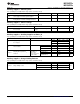
PARAMETER TEST CONDITIONS V
CC
MIN TYP MAX UNIT
2.0 V 0
SOMI input data hold
t
HD,MI
ns
time
3.0 V 0
2.0 V 9
SIMO output data valid
t
VALID,MO
UCLK edge to SIMO valid, C
L
= 20 pF ns
time
(2)
3.0 V 5
2.0 V 0
SIMO output data hold
t
HD,MO
C
L
= 20 pF ns
time
(3)
3.0 V 0
(2) Specifies the time to drive the next valid data to the SIMO output after the output changing UCLK clock edge. See the timing diagrams
in Figure 15 and Figure 16.
(3) Specifies how long data on the SIMO output is valid after the output changing UCLK clock edge. Negative values indicate that the data
on the SIMO output can become invalid before the output changing clock edge observed on UCLK. See the timing diagrams in
Figure 15 and Figure 16.
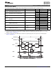
Figure 13. SPI Master Mode, CKPH = 0
Copyright © 2011–2013, Texas Instruments Incorporated Submit Documentation Feedback 65