
Datasheet


MSP430F673x
MSP430F672x
www.ti.com
SLAS731C –DECEMBER 2011–REVISED FEBRUARY 2013
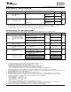
Inputs – Ports P1 and P2
(1)
over recommended ranges of supply voltage and operating free-air temperature (unless otherwise noted)
PARAMETER TEST CONDITIONS V
CC
MIN MAX UNIT
Port P1, P2: P1.x to P2.x, External trigger pulse width to
t
(int)
External interrupt timing
(2)
2.2 V/3 V 20 ns
set interrupt flag
(1) Some devices may contain additional ports with interrupts. See the block diagram and terminal function descriptions.
(2) An external signal sets the interrupt flag every time the minimum interrupt pulse width t
(int)
is met. It may be set by trigger signals shorter
than t
(int)
.
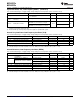
Leakage Current – General Purpose I/O
over recommended ranges of supply voltage and operating free-air temperature (unless otherwise noted)
PARAMETER TEST CONDITIONS V
CC
MIN MAX UNIT
I
lkg(Px.y)
High-impedance leakage current See
(1)(2)
1.8 V/3 V ±50 nA
(1) The leakage current is measured with V
SS
or V
CC
applied to the corresponding pin(s), unless otherwise noted.
(2) The leakage of the digital port pins is measured individually. The port pin is selected for input and the pullup/pulldown resistor is
disabled.
Outputs – General Purpose I/O (Full Drive Strength)
over recommended ranges of supply voltage and operating free-air temperature (unless otherwise noted)
PARAMETER TEST CONDITIONS V
CC
MIN MAX UNIT
I
(OHmax)
= –3 mA
(1)
V
CC
– 0.25 V
CC
1.8 V
I
(OHmax)
= –10 mA
(1)
V
CC
– 0.60 V
CC
V
OH
High-level output voltage V
I
(OHmax)
= –5 mA
(1)
V
CC
– 0.25 V
CC
3 V
I
(OHmax)
= –15 mA
(1)
V
CC
– 0.60 V
CC
I
(OLmax)
= 3 mA
(2)
V
SS
V
SS
+ 0.25
1.8 V
I
(OLmax)
= 10 mA
(3)
V
SS
V
SS
+ 0.60
V
OL
Low-level output voltage V
I
(OLmax)
= 5 mA
(2)
V
SS
V
SS
+ 0.25
3 V
I
(OLmax)
= 15 mA
(3)
V
SS
V
SS
+ 0.60
(1) The maximum total current, I
(OHmax)
, for all outputs combined should not exceed ±20 mA to hold the maximum voltage drop specified.
See Recommended Operating Conditions for more details.
(2) The maximum total current, I
(OLmax)
, for all outputs combined should not exceed ±48 mA to hold the maximum voltage drop specified.
(3) The maximum total current, I
(OLmax)
, for all outputs combined should not exceed ±100 mA to hold the maximum voltage drop specified.
Copyright © 2011–2013, Texas Instruments Incorporated Submit Documentation Feedback 51