
Datasheet


UCLK
CKPL =0
CKPL =1
SOMI
SIMO
t
SU,SIMO
t
HD,SIMO
t
VALID,SOMI
t
LOW/HIGH
1/f
UCxCLK
t
LOW/HIGH
t
DIS
t
ACC
STE
t
STE,LEAD
t
STE,LAG
UCMODEx=01
UCMODEx=10
MSP430F673x
MSP430F672x
www.ti.com
SLAS731C –DECEMBER 2011–REVISED FEBRUARY 2013
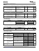
eUSCI (SPI Slave Mode)
over recommended ranges of supply voltage and operating free-air temperature (unless otherwise noted)
(1)
PARAMETER TEST CONDITIONS V
CC
MIN TYP MAX UNIT
2.0 V 4
t
STE,LEAD
STE lead time, STE active to clock ns
3.0 V 3
2.0 V 0
t
STE,LAG
STE lag time, Last clock to STE inactive ns
3.0 V 0
2.0 V 46
t
STE,ACC
STE access time, STE active to SOMI data out ns
3.0 V 24
2.0 V 38
STE disable time, STE inactive to SOMI high
t
STE,DIS
ns
impedance
3.0 V 25
2.0 V 2
t
SU,SI
SIMO input data setup time ns
3.0 V 1
2.0 V 2
t
HD,SI
SIMO input data hold time ns
3.0 V 2
2.0 V 55
UCLK edge to SOMI valid,
t
VALID,SO
SOMI output data valid time
(2)
ns
C
L
= 20 pF
3.0 V 32
2.0 V 24
t
HD,SO
SOMI output data hold time
(3)
C
L
= 20 pF ns
3.0 V 16
(1) f
UCxCLK
= 1/2t
LO/HI
with tL
O/HI
= max(t
VALID,MO(Master)
+ t
SU,SI(eUSCI)
, t
SU,MI(Master)
+ t
VALID,SO(eUSCI)
).
For the master's parameters t
SU,MI(Master)
and t
VALID,MO(Master)
refer to the SPI parameters of the attached slave.
(2) Specifies the time to drive the next valid data to the SOMI output after the output changing UCLK clock edge. Refer to the timing
diagrams in Figure 15 and Figure 16.
(3) Specifies how long data on the SOMI output is valid after the output changing UCLK clock edge. Refer to the timing diagrams
inFigure 15 and Figure 16.
Figure 15. SPI Slave Mode, CKPH = 0
Copyright © 2011–2013, Texas Instruments Incorporated Submit Documentation Feedback 67