
Datasheet


MSP430F6638, MSP430F6637, MSP430F6636
MSP430F6635, MSP430F6634, MSP430F6633
MSP430F6632, MSP430F6631, MSP430F6630
www.ti.com
SLAS566D –JUNE 2010–REVISED AUGUST 2013
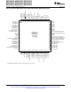
Table 2. Terminal Functions
TERMINAL
NO. I/O
(1)
DESCRIPTION
NAME
PZ ZQW
General-purpose digital I/O
P6.4/CB4/A4 1 A1 I/O
Comparator_B input CB4
Analog input A4 – ADC(not available on F6632, F6631, F6630 devices)
General-purpose digital I/O
P6.5/CB5/A5 2 B2 I/O
Comparator_B input CB5
Analog input A5 – ADC(not available on F6632, F6631, F6630 devices)
General-purpose digital I/O
Comparator_B input CB6
P6.6/CB6/A6/DAC0 3 B1 I/O
Analog input A6 – ADC (not available on F6632, F6631, F6630 devices)
DAC12.0 output (not available on F6635, F6634, F6633, F6632, F6631, F6630
devices)
General-purpose digital I/O
Comparator_B input CB7
P6.7/CB7/A7/DAC1 4 C2 I/O
Analog input A7 – ADC (not available on F6632, F6631, F6630 devices)
DAC12.1 output (not available on F6635, F6634, F6633, F6632, F6631, F6630
devices)
General-purpose digital I/O
P7.4/CB8/A12 5 C1 I/O
Comparator_B input CB8
Analog input A12 –ADC (not available on F6632, F6631, F6630 devices)
General-purpose digital I/O
P7.5/CB9/A13 6 C3 I/O
Comparator_B input CB9
Analog input A13 – ADC (not available on F6632, F6631, F6630 devices)
General-purpose digital I/O
Comparator_B input CB10
P7.6/CB10/A14/DAC0 7 D2 I/O
Analog input A14 – ADC (not available on F6632, F6631, F6630 devices)
DAC12.0 output (not available on F6635, F6634, F6633, F6632, F6631, F6630
devices)
General-purpose digital I/O
Comparator_B input CB11
P7.7/CB11/A15/DAC1 8 D1 I/O
Analog input A15 – ADC (not available on F6632, F6631, F6630 devices)
DAC12.1 output (not available on F6635, F6634, F6633, F6632, F6631, F6630
devices)
General-purpose digital I/O
P5.0/VREF+/VeREF+ 9 D4 I/O
Output of reference voltage to the ADC
Input for an external reference voltage to the ADC
General-purpose digital I/O
P5.1/VREF-/VeREF- 10 E4 I/O
Negative terminal for the ADC's reference voltage for both sources, the internal
reference voltage, or an external applied reference voltage
E1,
AVCC1 11 Analog power supply
E2
AVSS1 12 F2 Analog ground supply
XIN 13 F1 I Input terminal for crystal oscillator XT1
XOUT 14 G1 O Output terminal of crystal oscillator XT1
AVSS2 15 G2 Analog ground supply
(1) I = input, O = output, N/A = not available on this package offering
Copyright © 2010–2013, Texas Instruments Incorporated Submit Documentation Feedback 9
Product Folder Links: MSP430F6638 MSP430F6637 MSP430F6636 MSP430F6635 MSP430F6634 MSP430F6633
MSP430F6632 MSP430F6631 MSP430F6630