
Datasheet


MSP430F6638, MSP430F6637, MSP430F6636
MSP430F6635, MSP430F6634, MSP430F6633
MSP430F6632, MSP430F6631, MSP430F6630
www.ti.com
SLAS566D –JUNE 2010–REVISED AUGUST 2013
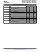
Table 54. Port P1 (P1.0 to P1.7) Pin Functions
CONTROL BITS/SIGNALS
(1)
PIN NAME (P1.x) x FUNCTION
P1DIR.x P1SEL.x LCDS32...39
P1.0/TA0CLK/ACLK/ 0 P1.0 (I/O) I: 0; O: 1 0 0
S39
Timer TA0.TA0CLK 0 1 0
ACLK 1 1 0
S39 X X 1
P1.1/TA0.0/S38 1 P1.1 (I/O) I: 0; O: 1 0 0
Timer TA0.CCI0A capture input 0 1 0
Timer TA0.0 output 1 1 0
S38 X X 1
P1.2/TA0.1/S37 2 P1.2 (I/O) I: 0; O: 1 0 0
Timer TA0.CCI1A capture input 0 1 0
Timer TA0.1 output 1 1 0
S37 X X 1
P1.3/TA0.2/S36 3 P1.3 (I/O) I: 0; O: 1 0 0
Timer TA0.CCI2A capture input 0 1 0
Timer TA0.2 output 1 1 0
S36 X X 1
P1.4/TA0.3/S35 4 P1.4 (I/O) I: 0; O: 1 0 0
Timer TA0.CCI3A capture input 0 1 0
Timer TA0.3 output 1 1 0
S35 X X 1
P1.5/TA0.4/S34 5 P1.5 (I/O) I: 0; O: 1 0 0
Timer TA0.CCI4A capture input 0 1 0
Timer TA0.4 output 1 1 0
S34 X X 1
P1.6/TA0.1/S33 6 P1.6 (I/O) I: 0; O: 1 0 0
Timer TA0.CCI1B capture input 0 1 0
Timer TA0.1 output 1 1 0
S33 X X 1
P1.7/TA0.2/S32 7 P1.7 (I/O) I: 0; O: 1 0 0
Timer TA0.CCI2B capture input 0 1 0
Timer TA0.2 output 1 1 0
S32 X X 1
(1) X = Don't care
Copyright © 2010–2013, Texas Instruments Incorporated Submit Documentation Feedback 85
Product Folder Links: MSP430F6638 MSP430F6637 MSP430F6636 MSP430F6635 MSP430F6634 MSP430F6633
MSP430F6632 MSP430F6631 MSP430F6630