
Datasheet


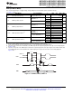


t
SU,MI
t
HD,MI
UCLK
SOMI
SIMO
t
VALID,MO
t
HD,MO
CKPL =0
CKPL =1
t
LO/HI
t
LO/HI
1/f
UCxCLK
MSP430F6638, MSP430F6637, MSP430F6636
MSP430F6635, MSP430F6634, MSP430F6633
MSP430F6632, MSP430F6631, MSP430F6630
www.ti.com
SLAS566D –JUNE 2010–REVISED AUGUST 2013
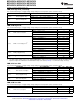
USCI (SPI Master Mode)
over recommended ranges of supply voltage and operating free-air temperature (unless otherwise noted)
(1)
(see Figure 12 and )
PARAMETER TEST CONDITIONS V
CC
MIN TYP MAX UNIT
SMCLK, ACLK,
f
USCI
USCI input clock frequency f
SYSTEM
MHz
Duty cycle = 50% ± 10%
1.8 V 55
PMMCOREV = 0 ns
3 V 38
t
SU,MI
SOMI input data setup time
2.4 V 30
PMMCOREV = 3 ns
3 V 25
1.8 V 0
PMMCOREV = 0 ns
3 V 0
t
HD,MI
SOMI input data hold time
2.4 V 0
PMMCOREV = 3 ns
3 V 0
UCLK edge to SIMO valid, 1.8 V 20
C
L
= 20 pF, ns
3 V 18
PMMCOREV = 0
t
VALID,MO
SIMO output data valid time
(2)
2.4 V 16
UCLK edge to SIMO valid,
ns
C
L
= 20 pF, PMMCOREV = 3
3 V 15
1.8 V -10
C
L
= 20 pF, PMMCOREV = 0 ns
3 V -8
t
HD,MO
SIMO output data hold time
(3)
2.4 V -10
C
L
= 20 pF, PMMCOREV = 3 ns
3 V -8
(1) f
UCxCLK
= 1/2t
LO/HI
with t
LO/HI
≥ max(t
VALID,MO(USCI)
+ t
SU,SI(Slave)
, t
SU,MI(USCI)
+ t
VALID,SO(Slave)
).
For the slave's parameters t
SU,SI(Slave)
and t
VALID,SO(Slave)
, see the SPI parameters of the attached slave.
(2) Specifies the time to drive the next valid data to the SIMO output after the output changing UCLK clock edge. See the timing diagrams
in Figure 12 and .
(3) Specifies how long data on the SIMO output is valid after the output changing UCLK clock edge. Negative values indicate that the data
on the SIMO output can become invalid before the output changing clock edge observed on UCLK. See the timing diagrams in
Figure 12 and .
Figure 12. SPI Master Mode, CKPH = 0
Copyright © 2010–2013, Texas Instruments Incorporated Submit Documentation Feedback 65
Product Folder Links: MSP430F6638 MSP430F6637 MSP430F6636 MSP430F6635 MSP430F6634 MSP430F6633
MSP430F6632 MSP430F6631 MSP430F6630