
Datasheet


MSP430F6638, MSP430F6637, MSP430F6636
MSP430F6635, MSP430F6634, MSP430F6633
MSP430F6632, MSP430F6631, MSP430F6630
www.ti.com
SLAS566D –JUNE 2010–REVISED AUGUST 2013
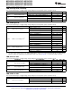
PMM, SVM Low Side (continued)
over recommended ranges of supply voltage and operating free-air temperature (unless otherwise noted)
PARAMETER TEST CONDITIONS MIN TYP MAX UNIT
SVMLE = 1, dV
CORE
/dt = 10 mV/µs, SVMLFP = 1 2.5
t
pd(SVML)
SVM
L
propagation delay µs
SVMLE = 1, dV
CORE
/dt = 1 mV/µs, SVMLFP = 0 20
SVMLE = 0→1, SVMLFP = 1 12.5
t
(SVML)
SVM
L
on/off delay time µs
SVMLE = 0→1, SVMLFP = 0 100
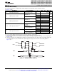
Wake-Up From Low-Power Modes and Reset
over recommended ranges of supply voltage and operating free-air temperature (unless otherwise noted)
PARAMETER TEST CONDITIONS MIN TYP MAX UNIT
f
MCLK
≥ 4 MHz 3 6.5
PMMCOREV = SVSMLRRL = n
Wake-up time from LPM2,
t
WAKE-UP-FAST
LPM3, or LPM4 to active (where n = 0, 1, 2, or 3), µs
1 MHz < f
MCLK
<
4 8.0
mode
(1)
SVSLFP = 1
4 MHz
PMMCOREV = SVSMLRRL = n
Wake-up time from LPM2,
(where n = 0, 1, 2, or 3),
t
WAKE-UP-SLOW
LPM3 or LPM4 to active 150 165 µs
mode
(2)
SVSLFP = 0
Wake-up time from LPM3.5 or
t
WAKE-UP-LPM5
2 3 ms
LPM4.5 to active mode
(3)
Wake-up time from RST or
t
WAKE-UP-RESET
2 3 ms
BOR event to active mode
(3)
(1) This value represents the time from the wakeup event to the first active edge of MCLK. The wakeup time depends on the performance
mode of the low-side supervisor (SVS
L
) and low side monitor (SVM
L
). Fastest wakeup times are possible with SVS
L
and SVM
L
in full
performance mode or disabled when operating in AM, LPM0, and LPM1. Various options are available for SVS
L
and SVM
L
while
operating in LPM2, LPM3, and LPM4. See the Power Management Module and Supply Voltage Supervisor chapter in the MSP430x5xx
and MSP430x6xx Family User's Guide (SLAU208).
(2) This value represents the time from the wakeup event to the first active edge of MCLK. The wakeup time depends on the performance
mode of the low-side supervisor (SVS
L
) and low side monitor (SVM
L
). In this case, the SVS
L
and SVM
L
are in normal mode (low current)
mode when operating in AM, LPM0, and LPM1. Various options are available for SVS
L
and SVM
L
while operating in LPM2, LPM3, and
LPM4. See the Power Management Module and Supply Voltage Supervisor chapter in the MSP430x5xx and MSP430x6xx Family User's
Guide (SLAU208).
(3) This value represents the time from the wakeup event to the reset vector execution.
Timer_A, Timers TA0, TA1, and TA2
over recommended ranges of supply voltage and operating free-air temperature (unless otherwise noted)
PARAMETER TEST CONDITIONS V
CC
MIN TYP MAX UNIT
Internal: SMCLK, ACLK
f
TA
Timer_A input clock frequency External: TACLK 1.8 V, 3 V 20 MHz
Duty cycle = 50% ± 10%
All capture inputs,
t
TA,cap
Timer_A capture timing Minimum pulse duration required for 1.8 V, 3 V 20 ns
capture
Timer_B, Timer TB0
over recommended ranges of supply voltage and operating free-air temperature (unless otherwise noted)
PARAMETER TEST CONDITIONS V
CC
MIN TYP MAX UNIT
Internal: SMCLK, ACLK
f
TB
Timer_B input clock frequency External: TBCLK 1.8 V, 3 V 20 MHz
Duty cycle = 50% ± 10%
All capture inputs,
t
TB,cap
Timer_B capture timing Minimum pulse duration required for 1.8 V, 3 V 20 ns
capture
Copyright © 2010–2013, Texas Instruments Incorporated Submit Documentation Feedback 63
Product Folder Links: MSP430F6638 MSP430F6637 MSP430F6636 MSP430F6635 MSP430F6634 MSP430F6633
MSP430F6632 MSP430F6631 MSP430F6630