
Datasheet


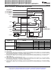


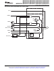

Table Of Contents
- Features
- Description
- Functional Block Diagram – MSP430F5529IPN, MSP430F5527IPN, MSP430F5525IPN, MSP430F5521IPN
- Pin Designation – MSP430F5529IPN, MSP430F5527IPN, MSP430F5525IPN, MSP430F5521IPN
- Functional Block Diagram – MSP430F5528IRGC, MSP430F5526IRGC, MSP430F5524IRGC, MSP430F5522IRGC MSP430F5528IZQE, MSP430F5526IZQE, MSP430F5524IZQE, MSP430F5522IZQE MSP430F5528IYFF, MSP430F5526IYFF, MSP430F5524IYFF
- Pin Designation – MSP430F5528IRGC, MSP430F5526IRGC, MSP430F5524IRGC, MSP430F5522IRGC
- Functional Block Diagram – MSP430F5519IPN, MSP430F5517IPN, MSP430F5515IPN
- Pin Designation – MSP430F5519IPN, MSP430F5517IPN, MSP430F5515IPN
- Functional Block Diagram – MSP430F5514IRGC, MSP430F5513IRGC, MSP430F5514IZQE, MSP430F5513IZQE
- Pin Designation – MSP430F5514IRGC, MSP430F5513IRGC
- Pin Designation – MSP430F5528IZQE, MSP430F5526IZQE, MSP430F5524IZQE, MSP430F5522IZQE, MSP430F5514IZQE, MSP430F5513IZQE
- Pin Designation – MSP430F5528IYFF, MSP430F5526IYFF, MSP430F5524IYFF
- Short-Form Description
- CPU
- Operating Modes
- Interrupt Vector Addresses
- Memory Organization
- Bootstrap Loader (BSL)
- JTAG Operation
- Flash Memory (Link to User's Guide)
- RAM Memory (Link to User's Guide)
- Peripherals
- Digital I/O (Link to User's Guide)
- Port Mapping Controller (Link to User's Guide)
- Oscillator and System Clock (Link to User's Guide)
- Power Management Module (PMM) (Link to User's Guide)
- Hardware Multiplier (Link to User's Guide)
- Real-Time Clock (RTC_A) (Link to User's Guide)
- Watchdog Timer (WDT_A) (Link to User's Guide)
- System Module (SYS) (Link to User's Guide)
- DMA Controller (Link to User's Guide)
- Universal Serial Communication Interface (USCI) (Links to User's Guide: UART Mode, SPI Mode, I2C Mode)
- TA0 (Link to User's Guide)
- TA1 (Link to User's Guide)
- TA2 (Link to User's Guide)
- TB0 (Link to User's Guide)
- Comparator_B (Link to User's Guide)
- ADC12_A (Link to User's Guide)
- CRC16 (Link to User's Guide)
- REF Voltage Reference (Link to User's Guide)
- USB Universal Serial Bus (Link to User's Guide)
- Embedded Emulation Module (EEM) (Link to User's Guide)
- Peripheral File Map
- Absolute Maximum Ratings
- Thermal Packaging Characteristics
- Recommended Operating Conditions
- Electrical Characteristics
- Active Mode Supply Current Into VCC Excluding External Current
- Low-Power Mode Supply Currents (Into VCC) Excluding External Current
- Schmitt-Trigger Inputs – General Purpose I/O (P1.0 to P1.7, P2.0 to P2.7, P3.0 to P3.7, P4.0 to P4.7) (P5.0 to P5.7, P6.0 to P6.7, P7.0 to P7.7, P8.0 to P8.2, PJ.0 to PJ.3, RST/NMI)
- Inputs – Ports P1 and P2 (P1.0 to P1.7, P2.0 to P2.7)
- Leakage Current – General Purpose I/O (P1.0 to P1.7, P2.0 to P2.7, P3.0 to P3.7, P4.0 to P4.7) (P5.0 to P5.7, P6.0 to P6.7, P7.0 to P7.7, P8.0 to P8.2, PJ.0 to PJ.3, RST/NMI)
- Outputs – General Purpose I/O (Full Drive Strength) (P1.0 to P1.7, P2.0 to P2.7, P3.0 to P3.7, P4.0 to P4.7) (P5.0 to P5.7, P6.0 to P6.7, P7.0 to P7.7, P8.0 to P8.2, PJ.0 to PJ.3)
- Outputs – General Purpose I/O (Reduced Drive Strength) (P1.0 to P1.7, P2.0 to P2.7, P3.0 to P3.7, P4.0 to P4.7) (P5.0 to P5.7, P6.0 to P6.7, P7.0 to P7.7, P8.0 to P8.2, PJ.0 to PJ.3)
- Output Frequency – General Purpose I/O (P1.0 to P1.7, P2.0 to P2.7, P3.0 to P3.7, P4.0 to P4.7) (P5.0 to P5.7, P6.0 to P6.7, P7.0 to P7.7, P8.0 to P8.2, PJ.0 to PJ.3)
- Typical Characteristics – Outputs, Reduced Drive Strength (PxDS.y = 0)
- Typical Characteristics – Outputs, Full Drive Strength (PxDS.y = 1)
- Crystal Oscillator, XT1, Low-Frequency Mode
- Crystal Oscillator, XT2
- Internal Very-Low-Power Low-Frequency Oscillator (VLO)
- Internal Reference, Low-Frequency Oscillator (REFO)
- DCO Frequency
- PMM, Brown-Out Reset (BOR)
- PMM, Core Voltage
- PMM, SVS High Side
- PMM, SVM High Side
- PMM, SVS Low Side
- PMM, SVM Low Side
- Wake-Up From Low-Power Modes and Reset
- Timer_A
- Timer_B
- USCI (UART Mode) Recommended Operating Conditions
- USCI (UART Mode)
- USCI (SPI Master Mode) Recommended Operating Conditions
- USCI (SPI Master Mode)
- USCI (SPI Slave Mode)
- USCI (I2C Mode)
- 12-Bit ADC, Power Supply and Input Range Conditions
- 12-Bit ADC, Timing Parameters
- 12-Bit ADC, Linearity Parameters Using an External Reference Voltage or AVCC as Reference Voltage
- 12-Bit ADC, Linearity Parameters Using the Internal Reference Voltage
- 12-Bit ADC, Temperature Sensor and Built-In VMID
- REF, External Reference
- REF, Built-In Reference
- Comparator_B
- Ports PU.0 and PU.1
- USB Output Ports DP and DM
- USB Input Ports DP and DM
- USB-PWR (USB Power System)
- USB-PLL (USB Phase Locked Loop)
- Flash Memory
- JTAG and Spy-Bi-Wire Interface
- Input/Output Schematics
- Port P1, P1.0 to P1.7, Input/Output With Schmitt Trigger
- Port P2, P2.0 to P2.7, Input/Output With Schmitt Trigger
- Port P3, P3.0 to P3.7, Input/Output With Schmitt Trigger
- Port P4, P4.0 to P4.7, Input/Output With Schmitt Trigger
- Port P5, P5.0 and P5.1, Input/Output With Schmitt Trigger
- Port P5, P5.2, Input/Output With Schmitt Trigger
- Port P5, P5.3, Input/Output With Schmitt Trigger
- Port P5, P5.6 to P5.7, Input/Output With Schmitt Trigger
- Port P6, P6.0 to P6.7, Input/Output With Schmitt Trigger
- Port P7, P7.0 to P7.3, Input/Output With Schmitt Trigger
- Port P7, P7.4 to P7.7, Input/Output With Schmitt Trigger
- Port P8, P8.0 to P8.2, Input/Output With Schmitt Trigger
- Port PU.0/DP, PU.1/DM, PUR USB Ports
- Port J, J.0 JTAG pin TDO, Input/Output With Schmitt Trigger or Output
- Port J, J.1 to J.3 JTAG pins TMS, TCK, TDI/TCLK, Input/Output With Schmitt Trigger or Output
- Device Descriptors (TLV)
- Revision History

P3.0/UCB0SIMO/UCB0SDA
P3.1/UCB0SOMI/UCB0SCL
P3.2/UCB0CLK/UCA0STE
P3.3/UCA0TXD/UCA0SIMO
P3.4/UCA0RXD/UCA0SOMI
P3.5/TB0.5
P3.6/TB0.6
P3.7/TB0OUTH/SVMOUT
Direction
0:Input
1:Output
P3SEL.x
1
0
P3DIR.x
P3IN.x
EN
Tomodule
1
0
Frommodule
P3OUT.x
1
0
DV
SS
DV
CC
P3REN.x
PadLogic
1
P3DS.x
0:Lowdrive
1:Highdrive
D
Frommodule
MSP430F5529, MSP430F5528, MSP430F5527, MSP430F5526
MSP430F5525, MSP430F5524, MSP430F5522, MSP430F5521
MSP430F5519, MSP430F5517, MSP430F5515, MSP430F5514, MSP430F5513
SLAS590L –MARCH 2009–REVISED MAY 2013
www.ti.com
Port P3, P3.0 to P3.7, Input/Output With Schmitt Trigger
Table 51. Port P3 (P3.0 to P3.7) Pin Functions
CONTROL BITS/SIGNALS
(1)
PIN NAME (P3.x) x FUNCTION
P3DIR.x P3SEL.x
P3.0/UCB0SIMO/UCB0SDA 0 P3.0 (I/O) I: 0; O: 1 0
UCB0SIMO/UCB0SDA
(2) (3)
X 1
P3.1/UCB0SOMI/UCB0SCL 1 P3.1 (I/O) I: 0; O: 1 0
UCB0SOMI/UCB0SCL
(2) (3)
X 1
P3.2/UCB0CLK/UCA0STE 2 P3.2 (I/O) I: 0; O: 1 0
UCB0CLK/UCA0STE
(2) (4)
X 1
P3.3/UCA0TXD/UCA0SIMO 3 P3.3 (I/O) I: 0; O: 1 0
UCA0TXD/UCA0SIMO
(2)
X 1
P3.4/UCA0RXD/UCA0SOMI 4 P3.4 (I/O) I: 0; O: 1 0
UCA0RXD/UCA0SOMI
(2)
X 1
P3.5/TB0.5
(5)
5 P3.5 (I/O) I: 0; O: 1 0
TB0.CCI5A 0 1
TB0.5 1 1
P3.6/TB0.6
(5)
6 P3.6 (I/O) I: 0; O: 1 0
TB0.CCI6A 0 1
TB0.6 1 1
P3.7/TB0OUTH/SVMOUT
(5)
7 P3.7 (I/O) I: 0; O: 1 0
TB0OUTH 0 1
SVMOUT 1 1
(1) X = Don't care
(2) The pin direction is controlled by the USCI module.
(3) If the I2C functionality is selected, the output drives only the logical 0 to V
SS
level.
(4) UCB0CLK function takes precedence over UCA0STE function. If the pin is required as UCB0CLK input or output, USCI A0 is forced to
3-wire SPI mode if 4-wire SPI mode is selected.
(5) F5529, F5527, F5525, F5521, F5519, F5517, F5515 devices only.
84 Submit Documentation Feedback Copyright © 2009–2013, Texas Instruments Incorporated
Product Folder Links: MSP430F5529 MSP430F5528 MSP430F5527 MSP430F5526 MSP430F5525 MSP430F5524
MSP430F5522 MSP430F5521 MSP430F5519 MSP430F5517 MSP430F5515 MSP430F5514 MSP430F5513