
Datasheet


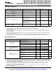


Table Of Contents
- Features
- Description
- Functional Block Diagram – MSP430F5529IPN, MSP430F5527IPN, MSP430F5525IPN, MSP430F5521IPN
- Pin Designation – MSP430F5529IPN, MSP430F5527IPN, MSP430F5525IPN, MSP430F5521IPN
- Functional Block Diagram – MSP430F5528IRGC, MSP430F5526IRGC, MSP430F5524IRGC, MSP430F5522IRGC MSP430F5528IZQE, MSP430F5526IZQE, MSP430F5524IZQE, MSP430F5522IZQE MSP430F5528IYFF, MSP430F5526IYFF, MSP430F5524IYFF
- Pin Designation – MSP430F5528IRGC, MSP430F5526IRGC, MSP430F5524IRGC, MSP430F5522IRGC
- Functional Block Diagram – MSP430F5519IPN, MSP430F5517IPN, MSP430F5515IPN
- Pin Designation – MSP430F5519IPN, MSP430F5517IPN, MSP430F5515IPN
- Functional Block Diagram – MSP430F5514IRGC, MSP430F5513IRGC, MSP430F5514IZQE, MSP430F5513IZQE
- Pin Designation – MSP430F5514IRGC, MSP430F5513IRGC
- Pin Designation – MSP430F5528IZQE, MSP430F5526IZQE, MSP430F5524IZQE, MSP430F5522IZQE, MSP430F5514IZQE, MSP430F5513IZQE
- Pin Designation – MSP430F5528IYFF, MSP430F5526IYFF, MSP430F5524IYFF
- Short-Form Description
- CPU
- Operating Modes
- Interrupt Vector Addresses
- Memory Organization
- Bootstrap Loader (BSL)
- JTAG Operation
- Flash Memory (Link to User's Guide)
- RAM Memory (Link to User's Guide)
- Peripherals
- Digital I/O (Link to User's Guide)
- Port Mapping Controller (Link to User's Guide)
- Oscillator and System Clock (Link to User's Guide)
- Power Management Module (PMM) (Link to User's Guide)
- Hardware Multiplier (Link to User's Guide)
- Real-Time Clock (RTC_A) (Link to User's Guide)
- Watchdog Timer (WDT_A) (Link to User's Guide)
- System Module (SYS) (Link to User's Guide)
- DMA Controller (Link to User's Guide)
- Universal Serial Communication Interface (USCI) (Links to User's Guide: UART Mode, SPI Mode, I2C Mode)
- TA0 (Link to User's Guide)
- TA1 (Link to User's Guide)
- TA2 (Link to User's Guide)
- TB0 (Link to User's Guide)
- Comparator_B (Link to User's Guide)
- ADC12_A (Link to User's Guide)
- CRC16 (Link to User's Guide)
- REF Voltage Reference (Link to User's Guide)
- USB Universal Serial Bus (Link to User's Guide)
- Embedded Emulation Module (EEM) (Link to User's Guide)
- Peripheral File Map
- Absolute Maximum Ratings
- Thermal Packaging Characteristics
- Recommended Operating Conditions
- Electrical Characteristics
- Active Mode Supply Current Into VCC Excluding External Current
- Low-Power Mode Supply Currents (Into VCC) Excluding External Current
- Schmitt-Trigger Inputs – General Purpose I/O (P1.0 to P1.7, P2.0 to P2.7, P3.0 to P3.7, P4.0 to P4.7) (P5.0 to P5.7, P6.0 to P6.7, P7.0 to P7.7, P8.0 to P8.2, PJ.0 to PJ.3, RST/NMI)
- Inputs – Ports P1 and P2 (P1.0 to P1.7, P2.0 to P2.7)
- Leakage Current – General Purpose I/O (P1.0 to P1.7, P2.0 to P2.7, P3.0 to P3.7, P4.0 to P4.7) (P5.0 to P5.7, P6.0 to P6.7, P7.0 to P7.7, P8.0 to P8.2, PJ.0 to PJ.3, RST/NMI)
- Outputs – General Purpose I/O (Full Drive Strength) (P1.0 to P1.7, P2.0 to P2.7, P3.0 to P3.7, P4.0 to P4.7) (P5.0 to P5.7, P6.0 to P6.7, P7.0 to P7.7, P8.0 to P8.2, PJ.0 to PJ.3)
- Outputs – General Purpose I/O (Reduced Drive Strength) (P1.0 to P1.7, P2.0 to P2.7, P3.0 to P3.7, P4.0 to P4.7) (P5.0 to P5.7, P6.0 to P6.7, P7.0 to P7.7, P8.0 to P8.2, PJ.0 to PJ.3)
- Output Frequency – General Purpose I/O (P1.0 to P1.7, P2.0 to P2.7, P3.0 to P3.7, P4.0 to P4.7) (P5.0 to P5.7, P6.0 to P6.7, P7.0 to P7.7, P8.0 to P8.2, PJ.0 to PJ.3)
- Typical Characteristics – Outputs, Reduced Drive Strength (PxDS.y = 0)
- Typical Characteristics – Outputs, Full Drive Strength (PxDS.y = 1)
- Crystal Oscillator, XT1, Low-Frequency Mode
- Crystal Oscillator, XT2
- Internal Very-Low-Power Low-Frequency Oscillator (VLO)
- Internal Reference, Low-Frequency Oscillator (REFO)
- DCO Frequency
- PMM, Brown-Out Reset (BOR)
- PMM, Core Voltage
- PMM, SVS High Side
- PMM, SVM High Side
- PMM, SVS Low Side
- PMM, SVM Low Side
- Wake-Up From Low-Power Modes and Reset
- Timer_A
- Timer_B
- USCI (UART Mode) Recommended Operating Conditions
- USCI (UART Mode)
- USCI (SPI Master Mode) Recommended Operating Conditions
- USCI (SPI Master Mode)
- USCI (SPI Slave Mode)
- USCI (I2C Mode)
- 12-Bit ADC, Power Supply and Input Range Conditions
- 12-Bit ADC, Timing Parameters
- 12-Bit ADC, Linearity Parameters Using an External Reference Voltage or AVCC as Reference Voltage
- 12-Bit ADC, Linearity Parameters Using the Internal Reference Voltage
- 12-Bit ADC, Temperature Sensor and Built-In VMID
- REF, External Reference
- REF, Built-In Reference
- Comparator_B
- Ports PU.0 and PU.1
- USB Output Ports DP and DM
- USB Input Ports DP and DM
- USB-PWR (USB Power System)
- USB-PLL (USB Phase Locked Loop)
- Flash Memory
- JTAG and Spy-Bi-Wire Interface
- Input/Output Schematics
- Port P1, P1.0 to P1.7, Input/Output With Schmitt Trigger
- Port P2, P2.0 to P2.7, Input/Output With Schmitt Trigger
- Port P3, P3.0 to P3.7, Input/Output With Schmitt Trigger
- Port P4, P4.0 to P4.7, Input/Output With Schmitt Trigger
- Port P5, P5.0 and P5.1, Input/Output With Schmitt Trigger
- Port P5, P5.2, Input/Output With Schmitt Trigger
- Port P5, P5.3, Input/Output With Schmitt Trigger
- Port P5, P5.6 to P5.7, Input/Output With Schmitt Trigger
- Port P6, P6.0 to P6.7, Input/Output With Schmitt Trigger
- Port P7, P7.0 to P7.3, Input/Output With Schmitt Trigger
- Port P7, P7.4 to P7.7, Input/Output With Schmitt Trigger
- Port P8, P8.0 to P8.2, Input/Output With Schmitt Trigger
- Port PU.0/DP, PU.1/DM, PUR USB Ports
- Port J, J.0 JTAG pin TDO, Input/Output With Schmitt Trigger or Output
- Port J, J.1 to J.3 JTAG pins TMS, TCK, TDI/TCLK, Input/Output With Schmitt Trigger or Output
- Device Descriptors (TLV)
- Revision History

MSP430F5529, MSP430F5528, MSP430F5527, MSP430F5526
MSP430F5525, MSP430F5524, MSP430F5522, MSP430F5521
MSP430F5519, MSP430F5517, MSP430F5515, MSP430F5514, MSP430F5513
SLAS590L –MARCH 2009–REVISED MAY 2013
www.ti.com
USB-PWR (USB Power System)
over recommended ranges of supply voltage and operating free-air temperature (unless otherwise noted)
PARAMETER TEST CONDITIONS V
CC
MIN TYP MAX UNIT
V
LAUNCH
V
BUS
detection threshold 3.75 V
V
BUS
USB bus voltage Normal operation 3.76 5.5 V
V
USB
USB LDO output voltage 3.003 3.3 3.597 V
V
18
Internal USB voltage
(1)
1.8 V
Maximum external current from VUSB
I
USB_EXT
USB LDO is on 12 mA
terminal
(2)
I
DET
USB LDO current overload detection
(3)
60 100 mA
USB LDO is on,
I
SUSPEND
Operating supply current into VBUS terminal
(4)
250 µA
USB PLL disabled
USB LDO is on,
Operating supply current into VBUS terminal, USB 1.8-V LDO is disabled,
I
USB_LDO
1.8 V, 3 V 60 µA
represents the current of the 3.3-V LDO only V
BUS
= 5.0 V,
USBDETEN = 0 or 1
USB LDO is disabled,
Operating supply current into VBUS terminal,
I
VBUS_DETE
USB 1.8-V LDO is disabled,
represents the current of the VBUS detection 1.8 V, 3 V 30 µA
CT
VBUS > V
LAUNCH
,
logic
USBDETEN = 1
C
BUS
VBUS terminal recommended capacitance 4.7 µF
C
USB
VUSB terminal recommended capacitance 220 nF
C
18
V18 terminal recommended capacitance 220 nF
Within 2%,
t
ENABLE
Settling time V
USB
and V
18
2 ms
recommended capacitances
RPUR Pullup resistance of PUR terminal
(5)
70 110 150 Ω
(1) This voltage is for internal uses only. No external DC loading should be applied.
(2) This represents additional current that can be supplied to the application from the VUSB terminal beyond the needs of the USB
operation.
(3) A current overload will be detected when the total current supplied from the USB LDO, including I
USB_EXT
, exceeds this value.
(4) Does not include current contribution of Rpu and Rpd as outlined in the USB specification.
(5) This value, in series with an external resistor between PUR and D+, produces the Rpu as outlined in the USB specification.
USB-PLL (USB Phase Locked Loop)
over recommended ranges of supply voltage and operating free-air temperature (unless otherwise noted)
PARAMETER TEST CONDITIONS V
CC
MIN TYP MAX UNIT
I
PLL
Operating supply current 7 mA
f
PLL
PLL frequency 48 MHz
f
UPD
PLL reference frequency 1.5 3 MHz
t
LOCK
PLL lock time 2 ms
t
Jitter
PLL jitter 1000 ps
78 Submit Documentation Feedback Copyright © 2009–2013, Texas Instruments Incorporated
Product Folder Links: MSP430F5529 MSP430F5528 MSP430F5527 MSP430F5526 MSP430F5525 MSP430F5524
MSP430F5522 MSP430F5521 MSP430F5519 MSP430F5517 MSP430F5515 MSP430F5514 MSP430F5513