
Datasheet


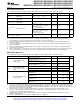


Table Of Contents
- Features
- Description
- Functional Block Diagram – MSP430F5529IPN, MSP430F5527IPN, MSP430F5525IPN, MSP430F5521IPN
- Pin Designation – MSP430F5529IPN, MSP430F5527IPN, MSP430F5525IPN, MSP430F5521IPN
- Functional Block Diagram – MSP430F5528IRGC, MSP430F5526IRGC, MSP430F5524IRGC, MSP430F5522IRGC MSP430F5528IZQE, MSP430F5526IZQE, MSP430F5524IZQE, MSP430F5522IZQE MSP430F5528IYFF, MSP430F5526IYFF, MSP430F5524IYFF
- Pin Designation – MSP430F5528IRGC, MSP430F5526IRGC, MSP430F5524IRGC, MSP430F5522IRGC
- Functional Block Diagram – MSP430F5519IPN, MSP430F5517IPN, MSP430F5515IPN
- Pin Designation – MSP430F5519IPN, MSP430F5517IPN, MSP430F5515IPN
- Functional Block Diagram – MSP430F5514IRGC, MSP430F5513IRGC, MSP430F5514IZQE, MSP430F5513IZQE
- Pin Designation – MSP430F5514IRGC, MSP430F5513IRGC
- Pin Designation – MSP430F5528IZQE, MSP430F5526IZQE, MSP430F5524IZQE, MSP430F5522IZQE, MSP430F5514IZQE, MSP430F5513IZQE
- Pin Designation – MSP430F5528IYFF, MSP430F5526IYFF, MSP430F5524IYFF
- Short-Form Description
- CPU
- Operating Modes
- Interrupt Vector Addresses
- Memory Organization
- Bootstrap Loader (BSL)
- JTAG Operation
- Flash Memory (Link to User's Guide)
- RAM Memory (Link to User's Guide)
- Peripherals
- Digital I/O (Link to User's Guide)
- Port Mapping Controller (Link to User's Guide)
- Oscillator and System Clock (Link to User's Guide)
- Power Management Module (PMM) (Link to User's Guide)
- Hardware Multiplier (Link to User's Guide)
- Real-Time Clock (RTC_A) (Link to User's Guide)
- Watchdog Timer (WDT_A) (Link to User's Guide)
- System Module (SYS) (Link to User's Guide)
- DMA Controller (Link to User's Guide)
- Universal Serial Communication Interface (USCI) (Links to User's Guide: UART Mode, SPI Mode, I2C Mode)
- TA0 (Link to User's Guide)
- TA1 (Link to User's Guide)
- TA2 (Link to User's Guide)
- TB0 (Link to User's Guide)
- Comparator_B (Link to User's Guide)
- ADC12_A (Link to User's Guide)
- CRC16 (Link to User's Guide)
- REF Voltage Reference (Link to User's Guide)
- USB Universal Serial Bus (Link to User's Guide)
- Embedded Emulation Module (EEM) (Link to User's Guide)
- Peripheral File Map
- Absolute Maximum Ratings
- Thermal Packaging Characteristics
- Recommended Operating Conditions
- Electrical Characteristics
- Active Mode Supply Current Into VCC Excluding External Current
- Low-Power Mode Supply Currents (Into VCC) Excluding External Current
- Schmitt-Trigger Inputs – General Purpose I/O (P1.0 to P1.7, P2.0 to P2.7, P3.0 to P3.7, P4.0 to P4.7) (P5.0 to P5.7, P6.0 to P6.7, P7.0 to P7.7, P8.0 to P8.2, PJ.0 to PJ.3, RST/NMI)
- Inputs – Ports P1 and P2 (P1.0 to P1.7, P2.0 to P2.7)
- Leakage Current – General Purpose I/O (P1.0 to P1.7, P2.0 to P2.7, P3.0 to P3.7, P4.0 to P4.7) (P5.0 to P5.7, P6.0 to P6.7, P7.0 to P7.7, P8.0 to P8.2, PJ.0 to PJ.3, RST/NMI)
- Outputs – General Purpose I/O (Full Drive Strength) (P1.0 to P1.7, P2.0 to P2.7, P3.0 to P3.7, P4.0 to P4.7) (P5.0 to P5.7, P6.0 to P6.7, P7.0 to P7.7, P8.0 to P8.2, PJ.0 to PJ.3)
- Outputs – General Purpose I/O (Reduced Drive Strength) (P1.0 to P1.7, P2.0 to P2.7, P3.0 to P3.7, P4.0 to P4.7) (P5.0 to P5.7, P6.0 to P6.7, P7.0 to P7.7, P8.0 to P8.2, PJ.0 to PJ.3)
- Output Frequency – General Purpose I/O (P1.0 to P1.7, P2.0 to P2.7, P3.0 to P3.7, P4.0 to P4.7) (P5.0 to P5.7, P6.0 to P6.7, P7.0 to P7.7, P8.0 to P8.2, PJ.0 to PJ.3)
- Typical Characteristics – Outputs, Reduced Drive Strength (PxDS.y = 0)
- Typical Characteristics – Outputs, Full Drive Strength (PxDS.y = 1)
- Crystal Oscillator, XT1, Low-Frequency Mode
- Crystal Oscillator, XT2
- Internal Very-Low-Power Low-Frequency Oscillator (VLO)
- Internal Reference, Low-Frequency Oscillator (REFO)
- DCO Frequency
- PMM, Brown-Out Reset (BOR)
- PMM, Core Voltage
- PMM, SVS High Side
- PMM, SVM High Side
- PMM, SVS Low Side
- PMM, SVM Low Side
- Wake-Up From Low-Power Modes and Reset
- Timer_A
- Timer_B
- USCI (UART Mode) Recommended Operating Conditions
- USCI (UART Mode)
- USCI (SPI Master Mode) Recommended Operating Conditions
- USCI (SPI Master Mode)
- USCI (SPI Slave Mode)
- USCI (I2C Mode)
- 12-Bit ADC, Power Supply and Input Range Conditions
- 12-Bit ADC, Timing Parameters
- 12-Bit ADC, Linearity Parameters Using an External Reference Voltage or AVCC as Reference Voltage
- 12-Bit ADC, Linearity Parameters Using the Internal Reference Voltage
- 12-Bit ADC, Temperature Sensor and Built-In VMID
- REF, External Reference
- REF, Built-In Reference
- Comparator_B
- Ports PU.0 and PU.1
- USB Output Ports DP and DM
- USB Input Ports DP and DM
- USB-PWR (USB Power System)
- USB-PLL (USB Phase Locked Loop)
- Flash Memory
- JTAG and Spy-Bi-Wire Interface
- Input/Output Schematics
- Port P1, P1.0 to P1.7, Input/Output With Schmitt Trigger
- Port P2, P2.0 to P2.7, Input/Output With Schmitt Trigger
- Port P3, P3.0 to P3.7, Input/Output With Schmitt Trigger
- Port P4, P4.0 to P4.7, Input/Output With Schmitt Trigger
- Port P5, P5.0 and P5.1, Input/Output With Schmitt Trigger
- Port P5, P5.2, Input/Output With Schmitt Trigger
- Port P5, P5.3, Input/Output With Schmitt Trigger
- Port P5, P5.6 to P5.7, Input/Output With Schmitt Trigger
- Port P6, P6.0 to P6.7, Input/Output With Schmitt Trigger
- Port P7, P7.0 to P7.3, Input/Output With Schmitt Trigger
- Port P7, P7.4 to P7.7, Input/Output With Schmitt Trigger
- Port P8, P8.0 to P8.2, Input/Output With Schmitt Trigger
- Port PU.0/DP, PU.1/DM, PUR USB Ports
- Port J, J.0 JTAG pin TDO, Input/Output With Schmitt Trigger or Output
- Port J, J.1 to J.3 JTAG pins TMS, TCK, TDI/TCLK, Input/Output With Schmitt Trigger or Output
- Device Descriptors (TLV)
- Revision History

MSP430F5529, MSP430F5528, MSP430F5527, MSP430F5526
MSP430F5525, MSP430F5524, MSP430F5522, MSP430F5521
MSP430F5519, MSP430F5517, MSP430F5515, MSP430F5514, MSP430F5513
www.ti.com
SLAS590L –MARCH 2009–REVISED MAY 2013
Comparator_B
over recommended ranges of supply voltage and operating free-air temperature (unless otherwise noted)
PARAMETER TEST CONDITIONS V
CC
MIN TYP MAX UNIT
V
CC
Supply voltage 1.8 3.6 V
1.8 V 40
CBPWRMD = 00 2.2 V 30 50
Comparator operating supply
I
AVCC_COMP
current into AVCC, excludes 3.0 V 40 65 µA
reference resistor ladder
CBPWRMD = 01 2.2 V, 3 V 10 30
CBPWRMD = 10 2.2 V, 3 V 0.1 0.5
Quiescent current of local
CBREFACC = 1,
I
AVCC_REF
reference voltage amplifier into 22 µA
CBREFLx = 01
AVCC
V
IC
Common mode input range 0 V
CC
-1 V
CBPWRMD = 00 -20 20 mV
V
OFFSET
Input offset voltage
CBPWRMD = 01, 10 -10 10 mV
C
IN
Input capacitance 5 pF
ON - switch closed 3 4 kΩ
R
SIN
Series input resistance
OFF - switch open 30 MΩ
CBPWRMD = 00, CBF = 0 450 ns
Propagation delay, response
t
PD
CBPWRMD = 01, CBF = 0 600 ns
time
CBPWRMD = 10, CBF = 0 50 µs
CBPWRMD = 00, CBON = 1,
0.35 0.6 1.0 µs
CBF = 1, CBFDLY = 00
CBPWRMD = 00, CBON = 1,
0.6 1.0 1.8 µs
CBF = 1, CBFDLY = 01
Propagation delay with filter
t
PD,filter
active
CBPWRMD = 00, CBON = 1,
1.0 1.8 3.4 µs
CBF = 1, CBFDLY = 10
CBPWRMD = 00, CBON = 1,
1.8 3.4 6.5 µs
CBF = 1, CBFDLY = 11
Comparator enable time, CBON = 0 to CBON = 1,
t
EN_CMP
1 2 µs
settling time CBPWRMD = 00, 01, 10
t
EN_REF
Resistor reference enable time CBON = 0 to CBON = 1 1 1.5 µs
VIN × VIN × VIN ×
Reference voltage for a given VIN = reference into resistor
V
CB_REF
(n+0.5) (n+1) (n+1.5) V
tap ladder (n = 0 to 31)
/ 32 / 32 / 32
Ports PU.0 and PU.1
over recommended ranges of supply voltage and operating free-air temperature (unless otherwise noted)
PARAMETER TEST CONDITIONS V
CC
MIN TYP MAX UNIT
V
USB
= 3.3 V ± 10%, I
OH
= -25 mA,
V
OH
High-level output voltage 2.4 V
See Figure 18 for typical characteristics
V
USB
= 3.3 V ± 10%, I
OL
= 25 mA,
V
OL
Low-level output voltage 0.4 V
See Figure 17 for typical characteristics
V
USB
= 3.3 V ± 10%,
V
IH
High-level input voltage 2.0 V
See Figure 19 for typical characteristics
V
USB
= 3.3 V ± 10%,
V
IL
Low-level input voltage 0.8 V
See Figure 19 for typical characteristics
Copyright © 2009–2013, Texas Instruments Incorporated Submit Documentation Feedback 75
Product Folder Links: MSP430F5529 MSP430F5528 MSP430F5527 MSP430F5526 MSP430F5525 MSP430F5524
MSP430F5522 MSP430F5521 MSP430F5519 MSP430F5517 MSP430F5515 MSP430F5514 MSP430F5513