
Datasheet


MSP430F5529, MSP430F5528, MSP430F5527, MSP430F5526
MSP430F5525, MSP430F5524, MSP430F5522, MSP430F5521
MSP430F5519, MSP430F5517, MSP430F5515, MSP430F5514, MSP430F5513
www.ti.com
SLAS590L –MARCH 2009–REVISED MAY 2013
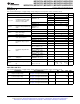
12-Bit ADC, Linearity Parameters Using an External Reference Voltage or AVCC as Reference
Voltage
over recommended ranges of supply voltage and operating free-air temperature (unless otherwise noted)
PARAMETER TEST CONDITIONS V
CC
MIN TYP MAX UNIT
1.4 V ≤ dVREF ≤ 1.6 V
(2)
±2.0
E
I
Integral linearity error
(1)
2.2 V, 3 V LSB
1.6 V < dVREF
(2)
±1.7
E
D
Differential linearity error
(1) (2)
2.2 V, 3 V ±1.0 LSB
dVREF ≤ 2.2 V
(2)
2.2 V, 3 V ±1.0 ±2.0
E
O
Offset error
(3)
LSB
dVREF > 2.2 V
(2)
2.2 V, 3 V ±1.0 ±2.0
E
G
Gain error
(3) (2)
2.2 V, 3 V ±1.0 ±2.0 LSB
dVREF ≤ 2.2 V
(2)
2.2 V, 3 V ±1.4 ±3.5
E
T
Total unadjusted error LSB
dVREF > 2.2 V
(2)
2.2 V, 3 V ±1.4 ±3.5
(1) Parameters are derived using the histogram method.
(2) The external reference voltage is selected by: SREF2 = 0 or 1, SREF1 = 1, SREF0 = 0. dVREF = V
R+
- V
R-
, V
R+
< AVCC, V
R-
> AVSS.
Unless otherwise mentioned, dVREF > 1.5 V. Impedance of the external reference voltage R < 100 Ω, and two decoupling capacitors,
10 µF and 100 nF, should be connected to VREF+ and VREF- to decouple the dynamic current. Also see the MSP430x5xx and
MSP430x6xx Family User's Guide (SLAU208).
(3) Parameters are derived using a best fit curve.
12-Bit ADC, Linearity Parameters Using the Internal Reference Voltage
over recommended ranges of supply voltage and operating free-air temperature (unless otherwise noted)
PARAMETER TEST CONDITIONS
(1)
V
CC
MIN TYP MAX UNIT
ADC12SR = 0, REFOUT = 1 f
ADC12CLK
= 4.0 MHz ±1.7
Integral linearity
E
I
2.2 V, 3 V LSB
error
(2)
ADC12SR = 0, REFOUT = 0 f
ADC12CLK
= 2.7 MHz ±2.5
ADC12SR = 0, REFOUT = 1 f
ADC12CLK
= 4.0 MHz -1.0 +2.0
Differential
E
D
ADC12SR = 0, REFOUT = 1 f
ADC12CLK
= 2.7 MHz 2.2 V, 3 V -1.0 +1.5 LSB
linearity error
(2)
ADC12SR = 0, REFOUT = 0 f
ADC12CLK
= 2.7 MHz -1.0 +2.5
ADC12SR = 0, REFOUT = 1 f
ADC12CLK
= 4.0 MHz ±1.0 ±2.0
E
O
Offset error
(3)
2.2 V, 3 V LSB
ADC12SR = 0, REFOUT = 0 f
ADC12CLK
= 2.7 MHz ±1.0 ±2.0
ADC12SR = 0, REFOUT = 1 f
ADC12CLK
= 4.0 MHz ±1.0 ±2.0 LSB
E
G
Gain error
(3)
2.2 V, 3 V
ADC12SR = 0, REFOUT = 0 f
ADC12CLK
= 2.7 MHz ±1.5%
(4)
VREF
ADC12SR = 0, REFOUT = 1 f
ADC12CLK
= 4.0 MHz ±1.4 ±3.5 LSB
Total unadjusted
E
T
2.2 V, 3 V
error
ADC12SR = 0, REFOUT = 0 f
ADC12CLK
= 2.7 MHz ±1.5%
(4)
VREF
(1) The internal reference voltage is selected by: SREF2 = 0 or 1, SREF1 = 1, SREF0 = 1. dVREF = V
R+
- V
R-
.
(2) Parameters are derived using the histogram method.
(3) Parameters are derived using a best fit curve.
(4) The gain error and total unadjusted error are dominated by the accuracy of the integrated reference module absolute accuracy. In this
mode the reference voltage used by the ADC12_A is not available on a pin.
Copyright © 2009–2013, Texas Instruments Incorporated Submit Documentation Feedback 71
Product Folder Links: MSP430F5529 MSP430F5528 MSP430F5527 MSP430F5526 MSP430F5525 MSP430F5524
MSP430F5522 MSP430F5521 MSP430F5519 MSP430F5517 MSP430F5515 MSP430F5514 MSP430F5513