
Datasheet

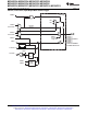


P4.0/P4MAP0
P4.1/P4MAP1
P4.2/P4MAP2
P4.3/P4MAP3
P4.4/P4MAP4
P4.5/P4MAP5
P4.6/P4MAP6
P4.7/P4MAP7
Direction
0:Input
1:Output
P4SEL.x
1
0
P4DIR.x
P4IN.x
EN
toPortMappingControl
1
0
fromPortMappingControl
P4OUT.x
1
0
DV
SS
DV
CC
P4REN.x
PadLogic
1
P4DS.x
0:Lowdrive
1:Highdrive
D
fromPortMappingControl
MSP430F5529, MSP430F5528, MSP430F5527, MSP430F5526
MSP430F5525, MSP430F5524, MSP430F5522, MSP430F5521
MSP430F5519, MSP430F5517, MSP430F5515, MSP430F5514, MSP430F5513
www.ti.com
SLAS590L –MARCH 2009–REVISED MAY 2013
Port P4, P4.0 to P4.7, Input/Output With Schmitt Trigger
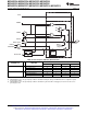
Table 52. Port P4 (P4.0 to P4.7) Pin Functions
CONTROL BITS/SIGNALS
PIN NAME (P4.x) x FUNCTION
P4DIR.x
(1)
P4SEL.x P4MAPx
P4.0/P4MAP0 0 P4.0 (I/O) I: 0; O: 1 0 X
Mapped secondary digital function X 1 ≤ 30
P4.1/P4MAP1 1 P4.1 (I/O) I: 0; O: 1 0 X
Mapped secondary digital function X 1 ≤ 30
P4.2/P4MAP2 2 P4.2 (I/O) I: 0; O: 1 0 X
Mapped secondary digital function X 1 ≤ 30
P4.3/P4MAP3 3 P4.3 (I/O) I: 0; O: 1 0 X
Mapped secondary digital function X 1 ≤ 30
P4.4/P4MAP4 4 P4.4 (I/O) I: 0; O: 1 0 X
Mapped secondary digital function X 1 ≤ 30
P4.5/P4MAP5 5 P4.5 (I/O) I: 0; O: 1 0 X
Mapped secondary digital function X 1 ≤ 30
P4.6/P4MAP6 6 P4.6 (I/O) I: 0; O: 1 0 X
Mapped secondary digital function X 1 ≤ 30
P4.7/P4MAP7 7 P4.7 (I/O) I: 0; O: 1 0 X
Mapped secondary digital function X 1 ≤ 30
(1) The direction of some mapped secondary functions are controlled directly by the module. See Table 10 for specific direction control
information of mapped secondary functions.
Copyright © 2009–2013, Texas Instruments Incorporated Submit Documentation Feedback 85
Product Folder Links: MSP430F5529 MSP430F5528 MSP430F5527 MSP430F5526 MSP430F5525 MSP430F5524
MSP430F5522 MSP430F5521 MSP430F5519 MSP430F5517 MSP430F5515 MSP430F5514 MSP430F5513