
Datasheet

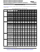


Table Of Contents
- Features
- Description
- Functional Block Diagram – MSP430F5529IPN, MSP430F5527IPN, MSP430F5525IPN, MSP430F5521IPN
- Pin Designation – MSP430F5529IPN, MSP430F5527IPN, MSP430F5525IPN, MSP430F5521IPN
- Functional Block Diagram – MSP430F5528IRGC, MSP430F5526IRGC, MSP430F5524IRGC, MSP430F5522IRGC MSP430F5528IZQE, MSP430F5526IZQE, MSP430F5524IZQE, MSP430F5522IZQE MSP430F5528IYFF, MSP430F5526IYFF, MSP430F5524IYFF
- Pin Designation – MSP430F5528IRGC, MSP430F5526IRGC, MSP430F5524IRGC, MSP430F5522IRGC
- Functional Block Diagram – MSP430F5519IPN, MSP430F5517IPN, MSP430F5515IPN
- Pin Designation – MSP430F5519IPN, MSP430F5517IPN, MSP430F5515IPN
- Functional Block Diagram – MSP430F5514IRGC, MSP430F5513IRGC, MSP430F5514IZQE, MSP430F5513IZQE
- Pin Designation – MSP430F5514IRGC, MSP430F5513IRGC
- Pin Designation – MSP430F5528IZQE, MSP430F5526IZQE, MSP430F5524IZQE, MSP430F5522IZQE, MSP430F5514IZQE, MSP430F5513IZQE
- Pin Designation – MSP430F5528IYFF, MSP430F5526IYFF, MSP430F5524IYFF
- Short-Form Description
- CPU
- Operating Modes
- Interrupt Vector Addresses
- Memory Organization
- Bootstrap Loader (BSL)
- JTAG Operation
- Flash Memory (Link to User's Guide)
- RAM Memory (Link to User's Guide)
- Peripherals
- Digital I/O (Link to User's Guide)
- Port Mapping Controller (Link to User's Guide)
- Oscillator and System Clock (Link to User's Guide)
- Power Management Module (PMM) (Link to User's Guide)
- Hardware Multiplier (Link to User's Guide)
- Real-Time Clock (RTC_A) (Link to User's Guide)
- Watchdog Timer (WDT_A) (Link to User's Guide)
- System Module (SYS) (Link to User's Guide)
- DMA Controller (Link to User's Guide)
- Universal Serial Communication Interface (USCI) (Links to User's Guide: UART Mode, SPI Mode, I2C Mode)
- TA0 (Link to User's Guide)
- TA1 (Link to User's Guide)
- TA2 (Link to User's Guide)
- TB0 (Link to User's Guide)
- Comparator_B (Link to User's Guide)
- ADC12_A (Link to User's Guide)
- CRC16 (Link to User's Guide)
- REF Voltage Reference (Link to User's Guide)
- USB Universal Serial Bus (Link to User's Guide)
- Embedded Emulation Module (EEM) (Link to User's Guide)
- Peripheral File Map
- Absolute Maximum Ratings
- Thermal Packaging Characteristics
- Recommended Operating Conditions
- Electrical Characteristics
- Active Mode Supply Current Into VCC Excluding External Current
- Low-Power Mode Supply Currents (Into VCC) Excluding External Current
- Schmitt-Trigger Inputs – General Purpose I/O (P1.0 to P1.7, P2.0 to P2.7, P3.0 to P3.7, P4.0 to P4.7) (P5.0 to P5.7, P6.0 to P6.7, P7.0 to P7.7, P8.0 to P8.2, PJ.0 to PJ.3, RST/NMI)
- Inputs – Ports P1 and P2 (P1.0 to P1.7, P2.0 to P2.7)
- Leakage Current – General Purpose I/O (P1.0 to P1.7, P2.0 to P2.7, P3.0 to P3.7, P4.0 to P4.7) (P5.0 to P5.7, P6.0 to P6.7, P7.0 to P7.7, P8.0 to P8.2, PJ.0 to PJ.3, RST/NMI)
- Outputs – General Purpose I/O (Full Drive Strength) (P1.0 to P1.7, P2.0 to P2.7, P3.0 to P3.7, P4.0 to P4.7) (P5.0 to P5.7, P6.0 to P6.7, P7.0 to P7.7, P8.0 to P8.2, PJ.0 to PJ.3)
- Outputs – General Purpose I/O (Reduced Drive Strength) (P1.0 to P1.7, P2.0 to P2.7, P3.0 to P3.7, P4.0 to P4.7) (P5.0 to P5.7, P6.0 to P6.7, P7.0 to P7.7, P8.0 to P8.2, PJ.0 to PJ.3)
- Output Frequency – General Purpose I/O (P1.0 to P1.7, P2.0 to P2.7, P3.0 to P3.7, P4.0 to P4.7) (P5.0 to P5.7, P6.0 to P6.7, P7.0 to P7.7, P8.0 to P8.2, PJ.0 to PJ.3)
- Typical Characteristics – Outputs, Reduced Drive Strength (PxDS.y = 0)
- Typical Characteristics – Outputs, Full Drive Strength (PxDS.y = 1)
- Crystal Oscillator, XT1, Low-Frequency Mode
- Crystal Oscillator, XT2
- Internal Very-Low-Power Low-Frequency Oscillator (VLO)
- Internal Reference, Low-Frequency Oscillator (REFO)
- DCO Frequency
- PMM, Brown-Out Reset (BOR)
- PMM, Core Voltage
- PMM, SVS High Side
- PMM, SVM High Side
- PMM, SVS Low Side
- PMM, SVM Low Side
- Wake-Up From Low-Power Modes and Reset
- Timer_A
- Timer_B
- USCI (UART Mode) Recommended Operating Conditions
- USCI (UART Mode)
- USCI (SPI Master Mode) Recommended Operating Conditions
- USCI (SPI Master Mode)
- USCI (SPI Slave Mode)
- USCI (I2C Mode)
- 12-Bit ADC, Power Supply and Input Range Conditions
- 12-Bit ADC, Timing Parameters
- 12-Bit ADC, Linearity Parameters Using an External Reference Voltage or AVCC as Reference Voltage
- 12-Bit ADC, Linearity Parameters Using the Internal Reference Voltage
- 12-Bit ADC, Temperature Sensor and Built-In VMID
- REF, External Reference
- REF, Built-In Reference
- Comparator_B
- Ports PU.0 and PU.1
- USB Output Ports DP and DM
- USB Input Ports DP and DM
- USB-PWR (USB Power System)
- USB-PLL (USB Phase Locked Loop)
- Flash Memory
- JTAG and Spy-Bi-Wire Interface
- Input/Output Schematics
- Port P1, P1.0 to P1.7, Input/Output With Schmitt Trigger
- Port P2, P2.0 to P2.7, Input/Output With Schmitt Trigger
- Port P3, P3.0 to P3.7, Input/Output With Schmitt Trigger
- Port P4, P4.0 to P4.7, Input/Output With Schmitt Trigger
- Port P5, P5.0 and P5.1, Input/Output With Schmitt Trigger
- Port P5, P5.2, Input/Output With Schmitt Trigger
- Port P5, P5.3, Input/Output With Schmitt Trigger
- Port P5, P5.6 to P5.7, Input/Output With Schmitt Trigger
- Port P6, P6.0 to P6.7, Input/Output With Schmitt Trigger
- Port P7, P7.0 to P7.3, Input/Output With Schmitt Trigger
- Port P7, P7.4 to P7.7, Input/Output With Schmitt Trigger
- Port P8, P8.0 to P8.2, Input/Output With Schmitt Trigger
- Port PU.0/DP, PU.1/DM, PUR USB Ports
- Port J, J.0 JTAG pin TDO, Input/Output With Schmitt Trigger or Output
- Port J, J.1 to J.3 JTAG pins TMS, TCK, TDI/TCLK, Input/Output With Schmitt Trigger or Output
- Device Descriptors (TLV)
- Revision History
MSP430F5529, MSP430F5528, MSP430F5527, MSP430F5526
MSP430F5525, MSP430F5524, MSP430F5522, MSP430F5521
MSP430F5519, MSP430F5517, MSP430F5515, MSP430F5514, MSP430F5513
www.ti.com
SLAS590L –MARCH 2009–REVISED MAY 2013
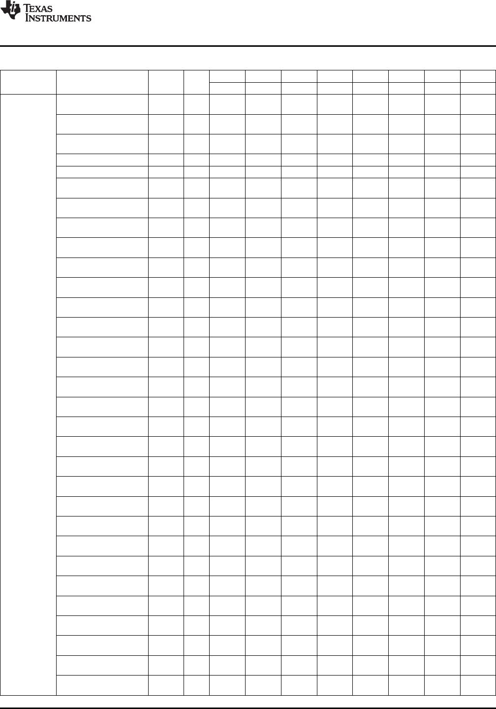
Table 65. MSP430F552x Device Descriptor Table
(1)
(continued)
F5529 F5528 F5527 F5526 F5525 F5524 F5522 F5521
Size
Description Address
bytes
Value Value Value Value Value Value Value Value
12h 12h 12h 12h 12h 12h 12h 12h
Memory 4 2
2Eh 2Eh 2Dh 2Dh 2Ch 2Ch 2Eh 2Dh
22h 22h 2Ah 2Ah 22h 22h 40h 2Ah
Memory 5 2
96h 96h 22h 22h 94h 94h 92h 40h
95h 95h
Memory 6 1/2 N/A N/A N/A N/A N/A 92h
92h 92h
delimiter 1 00h 00h 00h 00h 00h 00h 00h 00h
Peripheral count 1 21h 20h 21h 20h 21h 20h 20h 21h
00h 00h 00h 00h 00h 00h 00h 00h
MSP430CPUXV2 2
23h 23h 23h 23h 23h 23h 23h 23h
00h 00h 00h 00h 00h 00h 00h 00h
JTAG 2
09h 09h 09h 09h 09h 09h 09h 09h
00h 00h 00h 00h 00h 00h 00h 00h
SBW 2
0Fh 0Fh 0Fh 0Fh 0Fh 0Fh 0Fh 0Fh
00h 00h 00h 00h 00h 00h 00h 00h
EEM-L 2
05h 05h 05h 05h 05h 05h 05h 05h
00h 00h 00h 00h 00h 00h 00h 00h
TI BSL 2
FCh FCh FCh FCh FCh FCh FCh FCh
10h 10h 10h 10h 10h 10h 10h 10h
SFR 2
41h 41h 41h 41h 41h 41h 41h 41h
02h 02h 02h 02h 02h 02h 02h 02h
PMM 2
30h 30h 30h 30h 30h 30h 30h 30h
02h 02h 02h 02h 02h 02h 02h 02h
FCTL 2
38h 38h 38h 38h 38h 38h 38h 38h
01h 01h 01h 01h 01h 01h 01h 01h
CRC16 2
3Ch 3Ch 3Ch 3Ch 3Ch 3Ch 3Ch 3Ch
00h 00h 00h 00h 00h 00h 00h 00h
CRC16_RB 2
3Dh 3Dh 3Dh 3Dh 3Dh 3Dh 3Dh 3Dh
00h 00h 00h 00h 00h 00h 00h 00h
RAMCTL 2
44h 44h 44h 44h 44h 44h 44h 44h
00h 00h 00h 00h 00h 00h 00h 00h
WDT_A 2
40h 40h 40h 40h 40h 40h 40h 40h
01h 01h 01h 01h 01h 01h 01h 01h
UCS 2
48h 48h 48h 48h 48h 48h 48h 48h
02h 02h 02h 02h 02h 02h 02h 02h
SYS 2
42h 42h 42h 42h 42h 42h 42h 42h
03h 03h 03h 03h 03h 03h 03h 03h
REF 2
A0h A0h A0h A0h A0h A0h A0h A0h
01h 01h 01h 01h 01h 01h 01h 01h
Port Mapping 2
10h 10h 10h 10h 10h 10h 10h 10h
04h 04h 04h 04h 04h 04h 04h 04h
Port 1/2 2
51h 51h 51h 51h 51h 51h 51h 51h
02h 02h 02h 02h 02h 02h 02h 02h
Port 3/4 2
52h 52h 52h 52h 52h 52h 52h 52h
02h 02h 02h 02h 02h 02h 02h 02h
Port 5/6 2
53h 53h 53h 53h 53h 53h 53h 53h
02h 02h 02h 02h
Port 7/8 2 N/A N/A N/A N/A
54h 54h 54h 54h
0Ch 0Eh 0Ch 0Eh 0Ch 0Eh 0Eh 0Ch
JTAG 2
5Fh 5Fh 5Fh 5Fh 5Fh 5Fh 5Fh 5Fh
02h 02h 02h 02h 02h 02h 02h 02h
TA0 2
62h 62h 62h 62h 62h 62h 62h 62h
04h 04h 04h 04h 04h 04h 04h 04h
TA1 2
61h 61h 61h 61h 61h 61h 61h 61h
04h 04h 04h 04h 04h 04h 04h 04h
TB0 2
67h 67h 67h 67h 67h 67h 67h 67h
04h 04h 04h 04h 04h 04h 04h 04h
TA2 2
61h 61h 61h 61h 61h 61h 61h 61h
0Ah 0Ah 0Ah 0Ah 0Ah 0Ah 0Ah 0Ah
RTC 2
68h 68h 68h 68h 68h 68h 68h 68h
Copyright © 2009–2013, Texas Instruments Incorporated Submit Documentation Feedback 103
Product Folder Links: MSP430F5529 MSP430F5528 MSP430F5527 MSP430F5526 MSP430F5525 MSP430F5524
MSP430F5522 MSP430F5521 MSP430F5519 MSP430F5517 MSP430F5515 MSP430F5514 MSP430F5513