
Datasheet


P4.0/P4MAP0
P4.1/P4MAP1
P4.2/P4MAP2
P4.3/P4MAP3
P4.4/P4MAP4
P4.5/P4MAP5
P4.6/P4MAP6
P4.7/P4MAP7
Direction
0:Input
1:Output
P4SEL.x
1
0
P4DIR.x
P4IN.x
EN
toPortMappingControl
1
0
fromPortMappingControl
P4OUT.x
1
0
DV
SS
DV
CC
P4REN.x
PadLogic
1
P4DS.x
0:Lowdrive
1:Highdrive
D
fromPortMappingControl
MSP430F5510, MSP430F5509, MSP430F5508, MSP430F5507
MSP430F5506, MSP430F5505, MSP430F5504, MSP430F5503
MSP430F5502, MSP430F5501, MSP430F5500
www.ti.com
SLAS645I –JULY 2009–REVISED NOVEMBER 2013
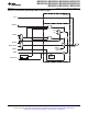
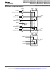
Port P4, P4.0 to P4.7, Input/Output With Schmitt Trigger
Table 50. Port P4 (P4.0 to P4.7) Pin Functions
CONTROL BITS OR SIGNALS
PIN NAME (P4.x) x FUNCTION
P4DIR.x
(1)
P4SEL.x P4MAPx
P4.0/P4MAP0 0 P4.0 (I/O) I: 0; O: 1 0 X
Mapped secondary digital function X 1 ≤ 30
P4.1/P4MAP1 1 P4.1 (I/O) I: 0; O: 1 0 X
Mapped secondary digital function X 1 ≤ 30
P4.2/P4MAP2 2 P4.2 (I/O) I: 0; O: 1 0 X
Mapped secondary digital function X 1 ≤ 30
P4.3/P4MAP3 3 P4.3 (I/O) I: 0; O: 1 0 X
Mapped secondary digital function X 1 ≤ 30
P4.4/P4MAP4 4 P4.4 (I/O) I: 0; O: 1 0 X
Mapped secondary digital function X 1 ≤ 30
P4.5/P4MAP5 5 P4.5 (I/O) I: 0; O: 1 0 X
Mapped secondary digital function X 1 ≤ 30
P4.6/P4MAP6 6 P4.6 (I/O) I: 0; O: 1 0 X
Mapped secondary digital function X 1 ≤ 30
P4.7/P4MAP7 7 P4.7 (I/O) I: 0; O: 1 0 X
Mapped secondary digital function X 1 ≤ 30
(1) The direction of some mapped secondary functions are controlled directly by the module. See Table 9 for specific direction control
information of mapped secondary functions.
Copyright © 2009–2013, Texas Instruments Incorporated Submit Documentation Feedback 81
Product Folder Links: MSP430F5510 MSP430F5509 MSP430F5508 MSP430F5507 MSP430F5506 MSP430F5505
MSP430F5504 MSP430F5503 MSP430F5502 MSP430F5501 MSP430F5500