
Datasheet

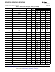


Table Of Contents
- Features
- Applications
- Description
- Development Tools Support
- Device and Development Tool Nomenclature
- Short-Form Description
- CPU
- Operating Modes
- Interrupt Vector Addresses
- Memory Organization
- Bootstrap Loader (BSL)
- JTAG Operation
- Flash Memory
- RAM Memory
- Peripherals
- Digital I/O
- Port Mapping Controller
- Oscillator and System Clock
- Power Management Module (PMM)
- Hardware Multiplier
- Real-Time Clock (RTC_A)
- Watchdog Timer (WDT_A)
- System Module (SYS)
- DMA Controller
- Universal Serial Communication Interface (USCI)
- TA0
- TA1
- TA2
- TB0
- Comparator_B
- ADC12_A
- CRC16
- REF Voltage Reference
- Embedded Emulation Module (EEM)
- Peripheral File Map
- Absolute Maximum Ratings
- Thermal Packaging Characteristics
- Recommended Operating Conditions
- Electrical Characteristics
- Active Mode Supply Current Into VCC Excluding External Current
- Low-Power Mode Supply Currents (Into VCC) Excluding External Current
- Schmitt-Trigger Inputs – General Purpose I/O (P1.0 to P1.7, P2.7, P3.0 to P3.4, P4.0 to P4.7) (P5.0 to P5.5, P5.7, P6.1 to P6.5, PJ.0 to PJ.3, RST/NMI)
- Inputs – Ports P1 and P2 (P1.0 to P1.7, P2.0 to P2.7)
- Leakage Current – General Purpose I/O (P1.0 to P1.7, P2.7, P3.0 to P3.4, P4.0 to P4.7) (P5.0 to P5.5, P5.7, P6.1 to P6.5, PJ.0 to PJ.3, RST/NMI)
- Outputs – General Purpose I/O (Full Drive Strength) (P1.0 to P1.7, P2.7, P3.0 to P3.4, P4.0 to P4.7) (P5.0 to P5.5, P5.7, P6.1 to P6.5, PJ.0 to PJ.3)
- Outputs – General Purpose I/O (Reduced Drive Strength) (P1.0 to P1.7, P2.7, P3.0 to P3.4, P4.0 to P4.7) (P5.0 to P5.5, P5.7, P6.1 to P6.5, PJ.0 to PJ.3)
- Output Frequency – General Purpose I/O (P1.0 to P1.7, P2.7, P3.0 to P3.4, P4.0 to P4.7) (P5.0 to P5.5, P5.7, P6.1 to P6.5, PJ.0 to PJ.3)
- Typical Characteristics – Outputs, Reduced Drive Strength (PxDS.y = 0)
- Typical Characteristics – Outputs, Full Drive Strength (PxDS.y = 1)
- Crystal Oscillator, XT1, Low-Frequency Mode
- Crystal Oscillator, XT2
- Internal Very-Low-Power Low-Frequency Oscillator (VLO)
- Internal Reference, Low-Frequency Oscillator (REFO)
- DCO Frequency
- PMM, Brown-Out Reset (BOR)
- PMM, Core Voltage
- PMM, SVS High Side
- PMM, SVM High Side
- PMM, SVS Low Side
- PMM, SVM Low Side
- Wake Up From Low Power Modes and Reset
- Timer_A
- Timer_B
- USCI (UART Mode) Recommended Operating Conditions
- USCI (UART Mode)
- USCI (SPI Master Mode) Recommended Operating Conditions
- USCI (SPI Master Mode)
- USCI (SPI Slave Mode)
- USCI (I2C Mode)
- 12-Bit ADC, Power Supply and Input Range Conditions
- 12-Bit ADC, Timing Parameters
- 12-Bit ADC, Linearity Parameters Using an External Reference Voltage or AVCC as Reference Voltage
- 12-Bit ADC, Linearity Parameters Using the Internal Reference Voltage
- 12-Bit ADC, Temperature Sensor and Built-In VMID
- REF, External Reference
- REF, Built-In Reference
- Comparator B
- Flash Memory
- JTAG and Spy-Bi-Wire Interface
- Input/Output Schematics
- Port P1, P1.0 to P1.7, Input/Output With Schmitt Trigger
- Port P2, P2.7, Input/Output With Schmitt Trigger
- Port P3, P3.0 to P3.4, Input/Output With Schmitt Trigger
- Port P4, P4.0 to P4.7, Input/Output With Schmitt Trigger
- Port P5, P5.0 and P5.1, Input/Output With Schmitt Trigger
- Port P5, P5.2, Input/Output With Schmitt Trigger
- Port P5, P5.3, Input/Output With Schmitt Trigger
- Port P5, P5.4 and P5.5 Input/Output With Schmitt Trigger
- Port P5, P5.7, Input/Output With Schmitt Trigger
- Port P6, P6.1 to P6.5, Input/Output With Schmitt Trigger
- Port J, J.0 JTAG pin TDO, Input/Output With Schmitt Trigger or Output
- Port J, J.1 to J.3 JTAG pins TMS, TCK, TDI/TCLK, Input/Output With Schmitt Trigger or Output
- Device Descriptors
- Revision History

PACKAGE OPTION ADDENDUM
www.ti.com
5-Jul-2013
Addendum-Page 1
PACKAGING INFORMATION
Orderable Device Status
(1)
Package Type Package
Drawing
Pins Package
Qty
Eco Plan
(2)
Lead/Ball Finish MSL Peak Temp
(3)
Op Temp (°C) Device Marking
(4/5)
Samples
MSP430F5340IRGZR ACTIVE VQFN RGZ 48 2500 Green (RoHS
& no Sb/Br)
CU NIPDAU Level-3-260C-168 HR M430
F5340
MSP430F5340IRGZT ACTIVE VQFN RGZ 48 250 Green (RoHS
& no Sb/Br)
CU NIPDAU Level-3-260C-168 HR M430
F5340
MSP430F5341IRGZR ACTIVE VQFN RGZ 48 2500 Green (RoHS
& no Sb/Br)
CU NIPDAU Level-3-260C-168 HR M430
F5341
MSP430F5341IRGZT ACTIVE VQFN RGZ 48 250 Green (RoHS
& no Sb/Br)
CU NIPDAU Level-3-260C-168 HR M430
F5341
MSP430F5342IRGZR ACTIVE VQFN RGZ 48 2500 Green (RoHS
& no Sb/Br)
CU NIPDAU Level-3-260C-168 HR M430
F5342
MSP430F5342IRGZT ACTIVE VQFN RGZ 48 250 Green (RoHS
& no Sb/Br)
CU NIPDAU Level-3-260C-168 HR M430
F5342
(1)
The marketing status values are defined as follows:
ACTIVE: Product device recommended for new designs.
LIFEBUY: TI has announced that the device will be discontinued, and a lifetime-buy period is in effect.
NRND: Not recommended for new designs. Device is in production to support existing customers, but TI does not recommend using this part in a new design.
PREVIEW: Device has been announced but is not in production. Samples may or may not be available.
OBSOLETE: TI has discontinued the production of the device.
(2)
Eco Plan - The planned eco-friendly classification: Pb-Free (RoHS), Pb-Free (RoHS Exempt), or Green (RoHS & no Sb/Br) - please check http://www.ti.com/productcontent for the latest availability
information and additional product content details.
TBD: The Pb-Free/Green conversion plan has not been defined.
Pb-Free (RoHS): TI's terms "Lead-Free" or "Pb-Free" mean semiconductor products that are compatible with the current RoHS requirements for all 6 substances, including the requirement that
lead not exceed 0.1% by weight in homogeneous materials. Where designed to be soldered at high temperatures, TI Pb-Free products are suitable for use in specified lead-free processes.
Pb-Free (RoHS Exempt): This component has a RoHS exemption for either 1) lead-based flip-chip solder bumps used between the die and package, or 2) lead-based die adhesive used between
the die and leadframe. The component is otherwise considered Pb-Free (RoHS compatible) as defined above.
Green (RoHS & no Sb/Br): TI defines "Green" to mean Pb-Free (RoHS compatible), and free of Bromine (Br) and Antimony (Sb) based flame retardants (Br or Sb do not exceed 0.1% by weight
in homogeneous material)
(3)
MSL, Peak Temp. -- The Moisture Sensitivity Level rating according to the JEDEC industry standard classifications, and peak solder temperature.
(4)
There may be additional marking, which relates to the logo, the lot trace code information, or the environmental category on the device.
(5)
Multiple Device Markings will be inside parentheses. Only one Device Marking contained in parentheses and separated by a "~" will appear on a device. If a line is indented then it is a continuation
of the previous line and the two combined represent the entire Device Marking for that device.