
Datasheet


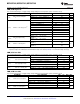
Table Of Contents
- Features
- Applications
- Description
- Development Tools Support
- Device and Development Tool Nomenclature
- Short-Form Description
- CPU
- Operating Modes
- Interrupt Vector Addresses
- Memory Organization
- Bootstrap Loader (BSL)
- JTAG Operation
- Flash Memory
- RAM Memory
- Peripherals
- Digital I/O
- Port Mapping Controller
- Oscillator and System Clock
- Power Management Module (PMM)
- Hardware Multiplier
- Real-Time Clock (RTC_A)
- Watchdog Timer (WDT_A)
- System Module (SYS)
- DMA Controller
- Universal Serial Communication Interface (USCI)
- TA0
- TA1
- TA2
- TB0
- Comparator_B
- ADC12_A
- CRC16
- REF Voltage Reference
- Embedded Emulation Module (EEM)
- Peripheral File Map
- Absolute Maximum Ratings
- Thermal Packaging Characteristics
- Recommended Operating Conditions
- Electrical Characteristics
- Active Mode Supply Current Into VCC Excluding External Current
- Low-Power Mode Supply Currents (Into VCC) Excluding External Current
- Schmitt-Trigger Inputs – General Purpose I/O (P1.0 to P1.7, P2.7, P3.0 to P3.4, P4.0 to P4.7) (P5.0 to P5.5, P5.7, P6.1 to P6.5, PJ.0 to PJ.3, RST/NMI)
- Inputs – Ports P1 and P2 (P1.0 to P1.7, P2.0 to P2.7)
- Leakage Current – General Purpose I/O (P1.0 to P1.7, P2.7, P3.0 to P3.4, P4.0 to P4.7) (P5.0 to P5.5, P5.7, P6.1 to P6.5, PJ.0 to PJ.3, RST/NMI)
- Outputs – General Purpose I/O (Full Drive Strength) (P1.0 to P1.7, P2.7, P3.0 to P3.4, P4.0 to P4.7) (P5.0 to P5.5, P5.7, P6.1 to P6.5, PJ.0 to PJ.3)
- Outputs – General Purpose I/O (Reduced Drive Strength) (P1.0 to P1.7, P2.7, P3.0 to P3.4, P4.0 to P4.7) (P5.0 to P5.5, P5.7, P6.1 to P6.5, PJ.0 to PJ.3)
- Output Frequency – General Purpose I/O (P1.0 to P1.7, P2.7, P3.0 to P3.4, P4.0 to P4.7) (P5.0 to P5.5, P5.7, P6.1 to P6.5, PJ.0 to PJ.3)
- Typical Characteristics – Outputs, Reduced Drive Strength (PxDS.y = 0)
- Typical Characteristics – Outputs, Full Drive Strength (PxDS.y = 1)
- Crystal Oscillator, XT1, Low-Frequency Mode
- Crystal Oscillator, XT2
- Internal Very-Low-Power Low-Frequency Oscillator (VLO)
- Internal Reference, Low-Frequency Oscillator (REFO)
- DCO Frequency
- PMM, Brown-Out Reset (BOR)
- PMM, Core Voltage
- PMM, SVS High Side
- PMM, SVM High Side
- PMM, SVS Low Side
- PMM, SVM Low Side
- Wake Up From Low Power Modes and Reset
- Timer_A
- Timer_B
- USCI (UART Mode) Recommended Operating Conditions
- USCI (UART Mode)
- USCI (SPI Master Mode) Recommended Operating Conditions
- USCI (SPI Master Mode)
- USCI (SPI Slave Mode)
- USCI (I2C Mode)
- 12-Bit ADC, Power Supply and Input Range Conditions
- 12-Bit ADC, Timing Parameters
- 12-Bit ADC, Linearity Parameters Using an External Reference Voltage or AVCC as Reference Voltage
- 12-Bit ADC, Linearity Parameters Using the Internal Reference Voltage
- 12-Bit ADC, Temperature Sensor and Built-In VMID
- REF, External Reference
- REF, Built-In Reference
- Comparator B
- Flash Memory
- JTAG and Spy-Bi-Wire Interface
- Input/Output Schematics
- Port P1, P1.0 to P1.7, Input/Output With Schmitt Trigger
- Port P2, P2.7, Input/Output With Schmitt Trigger
- Port P3, P3.0 to P3.4, Input/Output With Schmitt Trigger
- Port P4, P4.0 to P4.7, Input/Output With Schmitt Trigger
- Port P5, P5.0 and P5.1, Input/Output With Schmitt Trigger
- Port P5, P5.2, Input/Output With Schmitt Trigger
- Port P5, P5.3, Input/Output With Schmitt Trigger
- Port P5, P5.4 and P5.5 Input/Output With Schmitt Trigger
- Port P5, P5.7, Input/Output With Schmitt Trigger
- Port P6, P6.1 to P6.5, Input/Output With Schmitt Trigger
- Port J, J.0 JTAG pin TDO, Input/Output With Schmitt Trigger or Output
- Port J, J.1 to J.3 JTAG pins TMS, TCK, TDI/TCLK, Input/Output With Schmitt Trigger or Output
- Device Descriptors
- Revision History

MSP430F5342, MSP430F5341, MSP430F5340
SLAS706E –JULY 2011–REVISED AUGUST 2013
www.ti.com
PMM, Brown-Out Reset (BOR)
over recommended ranges of supply voltage and operating free-air temperature (unless otherwise noted)
PARAMETER TEST CONDITIONS MIN TYP MAX UNIT
V
(DVCC_BOR_IT–)
BOR
H
on voltage, DV
CC
falling level | dDV
CC
/d
t
| < 3 V/s 1.45 V
V
(DVCC_BOR_IT+)
BOR
H
off voltage, DV
CC
rising level | dDV
CC
/d
t
| < 3 V/s 0.80 1.30 1.50 V
V
(DVCC_BOR_hys)
BOR
H
hysteresis 60 250 mV
Pulse duration required at RST/NMI pin to accept a
t
RESET
2 µs
reset
PMM, Core Voltage
over recommended ranges of supply voltage and operating free-air temperature (unless otherwise noted)
PARAMETER TEST CONDITIONS MIN TYP MAX UNIT
V
CORE3
(AM) Core voltage, active mode, PMMCOREV = 3 2.4 V ≤ DV
CC
≤ 3.6 V 1.90 V
V
CORE2
(AM) Core voltage, active mode, PMMCOREV = 2 2.2 V ≤ DV
CC
≤ 3.6 V 1.80 V
V
CORE1
(AM) Core voltage, active mode, PMMCOREV = 1 2.0 V ≤ DV
CC
≤ 3.6 V 1.60 V
V
CORE0
(AM) Core voltage, active mode, PMMCOREV = 0 1.8 V ≤ DV
CC
≤ 3.6 V 1.40 V
V
CORE3
(LPM) Core voltage, low-current mode, PMMCOREV = 3 2.4 V ≤ DV
CC
≤ 3.6 V 1.94 V
V
CORE2
(LPM) Core voltage, low-current mode, PMMCOREV = 2 2.2 V ≤ DV
CC
≤ 3.6 V 1.84 V
V
CORE1
(LPM) Core voltage, low-current mode, PMMCOREV = 1 2.0 V ≤ DV
CC
≤ 3.6 V 1.64 V
V
CORE0
(LPM) Core voltage, low-current mode, PMMCOREV = 0 1.8 V ≤ DV
CC
≤ 3.6 V 1.44 V
48 Submit Documentation Feedback Copyright © 2011–2013, Texas Instruments Incorporated
Product Folder Links: MSP430F5342 MSP430F5341 MSP430F5340