
Datasheet


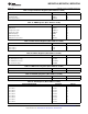


Table Of Contents
- Features
- Applications
- Description
- Development Tools Support
- Device and Development Tool Nomenclature
- Short-Form Description
- CPU
- Operating Modes
- Interrupt Vector Addresses
- Memory Organization
- Bootstrap Loader (BSL)
- JTAG Operation
- Flash Memory
- RAM Memory
- Peripherals
- Digital I/O
- Port Mapping Controller
- Oscillator and System Clock
- Power Management Module (PMM)
- Hardware Multiplier
- Real-Time Clock (RTC_A)
- Watchdog Timer (WDT_A)
- System Module (SYS)
- DMA Controller
- Universal Serial Communication Interface (USCI)
- TA0
- TA1
- TA2
- TB0
- Comparator_B
- ADC12_A
- CRC16
- REF Voltage Reference
- Embedded Emulation Module (EEM)
- Peripheral File Map
- Absolute Maximum Ratings
- Thermal Packaging Characteristics
- Recommended Operating Conditions
- Electrical Characteristics
- Active Mode Supply Current Into VCC Excluding External Current
- Low-Power Mode Supply Currents (Into VCC) Excluding External Current
- Schmitt-Trigger Inputs – General Purpose I/O (P1.0 to P1.7, P2.7, P3.0 to P3.4, P4.0 to P4.7) (P5.0 to P5.5, P5.7, P6.1 to P6.5, PJ.0 to PJ.3, RST/NMI)
- Inputs – Ports P1 and P2 (P1.0 to P1.7, P2.0 to P2.7)
- Leakage Current – General Purpose I/O (P1.0 to P1.7, P2.7, P3.0 to P3.4, P4.0 to P4.7) (P5.0 to P5.5, P5.7, P6.1 to P6.5, PJ.0 to PJ.3, RST/NMI)
- Outputs – General Purpose I/O (Full Drive Strength) (P1.0 to P1.7, P2.7, P3.0 to P3.4, P4.0 to P4.7) (P5.0 to P5.5, P5.7, P6.1 to P6.5, PJ.0 to PJ.3)
- Outputs – General Purpose I/O (Reduced Drive Strength) (P1.0 to P1.7, P2.7, P3.0 to P3.4, P4.0 to P4.7) (P5.0 to P5.5, P5.7, P6.1 to P6.5, PJ.0 to PJ.3)
- Output Frequency – General Purpose I/O (P1.0 to P1.7, P2.7, P3.0 to P3.4, P4.0 to P4.7) (P5.0 to P5.5, P5.7, P6.1 to P6.5, PJ.0 to PJ.3)
- Typical Characteristics – Outputs, Reduced Drive Strength (PxDS.y = 0)
- Typical Characteristics – Outputs, Full Drive Strength (PxDS.y = 1)
- Crystal Oscillator, XT1, Low-Frequency Mode
- Crystal Oscillator, XT2
- Internal Very-Low-Power Low-Frequency Oscillator (VLO)
- Internal Reference, Low-Frequency Oscillator (REFO)
- DCO Frequency
- PMM, Brown-Out Reset (BOR)
- PMM, Core Voltage
- PMM, SVS High Side
- PMM, SVM High Side
- PMM, SVS Low Side
- PMM, SVM Low Side
- Wake Up From Low Power Modes and Reset
- Timer_A
- Timer_B
- USCI (UART Mode) Recommended Operating Conditions
- USCI (UART Mode)
- USCI (SPI Master Mode) Recommended Operating Conditions
- USCI (SPI Master Mode)
- USCI (SPI Slave Mode)
- USCI (I2C Mode)
- 12-Bit ADC, Power Supply and Input Range Conditions
- 12-Bit ADC, Timing Parameters
- 12-Bit ADC, Linearity Parameters Using an External Reference Voltage or AVCC as Reference Voltage
- 12-Bit ADC, Linearity Parameters Using the Internal Reference Voltage
- 12-Bit ADC, Temperature Sensor and Built-In VMID
- REF, External Reference
- REF, Built-In Reference
- Comparator B
- Flash Memory
- JTAG and Spy-Bi-Wire Interface
- Input/Output Schematics
- Port P1, P1.0 to P1.7, Input/Output With Schmitt Trigger
- Port P2, P2.7, Input/Output With Schmitt Trigger
- Port P3, P3.0 to P3.4, Input/Output With Schmitt Trigger
- Port P4, P4.0 to P4.7, Input/Output With Schmitt Trigger
- Port P5, P5.0 and P5.1, Input/Output With Schmitt Trigger
- Port P5, P5.2, Input/Output With Schmitt Trigger
- Port P5, P5.3, Input/Output With Schmitt Trigger
- Port P5, P5.4 and P5.5 Input/Output With Schmitt Trigger
- Port P5, P5.7, Input/Output With Schmitt Trigger
- Port P6, P6.1 to P6.5, Input/Output With Schmitt Trigger
- Port J, J.0 JTAG pin TDO, Input/Output With Schmitt Trigger or Output
- Port J, J.1 to J.3 JTAG pins TMS, TCK, TDI/TCLK, Input/Output With Schmitt Trigger or Output
- Device Descriptors
- Revision History

MSP430F5342, MSP430F5341, MSP430F5340
www.ti.com
SLAS706E –JULY 2011–REVISED AUGUST 2013
TA1
TA1 is a 16-bit timer/counter (Timer_A type) with three capture/compare registers. It can support multiple
captures or compares, PWM outputs, and interval timing. It also has extensive interrupt capabilities. Interrupts
may be generated from the counter on overflow conditions and from each of the capture/compare registers.
Table 13. TA1 Signal Connections
INPUT PIN DEVICE INPUT MODULE INPUT MODULE DEVICE OUTPUT OUTPUT PIN
MODULE BLOCK
NUMBER SIGNAL SIGNAL OUTPUT SIGNAL SIGNAL NUMBER
19-P1.6 TA1CLK TACLK
ACLK (internal) ACLK
Timer NA NA
SMCLK (internal) SMCLK
19-P1.6 TA1CLK TACLK
20-P1.7 TA1.0 CCI0A 20-P1.7
DV
SS
CCI0B
CCR0 TA0 TA1.0
DV
SS
GND
DV
CC
V
CC
Not available TA1.1 CCI1A Not available
CBOUT (internal) CCI1B
CCR1 TA1 TA1.1
DV
SS
GND
DV
CC
V
CC
Not available TA1.2 CCI2A Not available
ACLK (internal) CCI2B
CCR2 TA2 TA1.2
DV
SS
GND
DV
CC
V
CC
TA2
TA2 is a 16-bit timer/counter (Timer_A type) with three capture/compare registers. It can support multiple
captures or compares, PWM outputs, and interval timing. It also has extensive interrupt capabilities. Interrupts
may be generated from the counter on overflow conditions and from each of the capture/compare registers.
Table 14. TA2 Signal Connections
INPUT PIN DEVICE INPUT MODULE INPUT MODULE DEVICE OUTPUT OUTPUT PIN
MODULE BLOCK
NUMBER SIGNAL SIGNAL OUTPUT SIGNAL SIGNAL NUMBER
Not available TA2CLK TACLK
ACLK (internal) ACLK
Timer NA NA
SMCLK (internal) SMCLK
Not available TA2CLK TACLK
Not available TA2.0 CCI0A Not available
DV
SS
CCI0B
CCR0 TA0 TA2.0
DV
SS
GND
DV
CC
V
CC
Not available TA2.1 CCI1A Not available
CBOUT (internal) CCI1B
CCR1 TA1 TA2.1
DV
SS
GND
DV
CC
V
CC
Not available TA2.2 CCI2A Not available
ACLK (internal) CCI2B
CCR2 TA2 TA2.2
DV
SS
GND
DV
CC
V
CC
Copyright © 2011–2013, Texas Instruments Incorporated Submit Documentation Feedback 21
Product Folder Links: MSP430F5342 MSP430F5341 MSP430F5340