
Datasheet


MSP430F532x
www.ti.com
SLAS678D –AUGUST 2010–REVISED FEBRUARY 2013
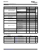
REF, Built-In Reference
over recommended ranges of supply voltage and operating free-air temperature (unless otherwise noted)
(1)
PARAMETER TEST CONDITIONS V
CC
MIN TYP MAX UNIT
REFVSEL = {2} for 2.5 V,
3 V 2.4625 2.50 2.5375
REFON = REFOUT = 1, I
VREF+
= 0 A
Positive built-in reference REFVSEL = {1} for 2.0 V,
V
REF+
3 V 1.9503 1.98 2.0097 V
voltage output REFON = REFOUT = 1, I
VREF+
= 0 A
REFVSEL = {0} for 1.5 V,
2.2 V, 3 V 1.4677 1.49 1.5124
REFON = REFOUT = 1, I
VREF+
= 0 A
REFVSEL = {0} for 1.5 V 2.2
AVCC minimum voltage,
AV
CC(min)
Positive built-in reference REFVSEL = {1} for 2.0 V 2.3 V
active
REFVSEL = {2} for 2.5 V 2.8
ADC12SR = 1
(4)
, REFON = 1, REFOUT = 0,
3 V 70 100 µA
REFBURST = 0
ADC12SR = 1
(4)
, REFON = 1, REFOUT = 1,
3 V 0.45 0.75 mA
REFBURST = 0
Operating supply current into
I
REF+
AVCC terminal
(2) (3)
ADC12SR = 0
(4)
, REFON = 1, REFOUT = 0,
3 V 210 310 µA
REFBURST = 0
ADC12SR = 0
(4)
, REFON = 1, REFOUT = 1,
3 V 0.95 1.7 mA
REFBURST = 0
REFVSEL = (0, 1, 2},
Load-current regulation, I
VREF+
= +10 µA/–1000 µA,
I
L(VREF+)
2500 µV/mA
VREF+ terminal
(5)
AVCC = AVCC(min) for each reference level,
REFVSEL = (0, 1, 2}, REFON = REFOUT = 1
Capacitance at VREF+
C
VREF+
REFON = REFOUT = 1 20 100 pF
terminals
I
VREF+
= 0 A,
Temperature coefficient of ppm/
TC
REF+
REFVSEL = (0, 1, 2}, REFON = 1, 30 50
built-in reference
(6)
°C
REFOUT = 0 or 1
AVCC = AVCC(min) - AVCC(max),
Power supply rejection ratio
PSRR_DC T
A
= 25°C, REFVSEL = (0, 1, 2}, REFON = 1, 120 300 µV/V
(DC)
REFOUT = 0 or 1
AVCC = AVCC(min) - AVCC(max),
Power supply rejection ratio T
A
= 25°C, f = 1 kHz, ΔVpp = 100 mV,
PSRR_AC 6.4 mV/V
(AC) REFVSEL = (0, 1, 2}, REFON = 1,
REFOUT = 0 or 1
AVCC = AVCC(min) - AVCC(max),
REFVSEL = (0, 1, 2}, REFOUT = 0, 75
REFON = 0 → 1
Settling time of reference
t
SETTLE
µs
AVCC = AVCC(min) - AVCC(max),
voltage
(7)
C
VREF
= C
VREF
(max),
75
REFVSEL = (0, 1, 2}, REFOUT = 1,
REFON = 0 → 1
(1) The reference is supplied to the ADC by the REF module and is buffered locally inside the ADC. The ADC uses two internal buffers, one
smaller and one larger for driving the V
REF+
terminal. When REFOUT = 1, the reference is available at the V
REF+
terminal, as well as,
used as the reference for the conversion and utilizes the larger buffer. When REFOUT = 0, the reference is only used as the reference
for the conversion and utilizes the smaller buffer.
(2) The internal reference current is supplied via terminal AVCC. Consumption is independent of the ADC12ON control bit, unless a
conversion is active. REFOUT = 0 represents the current contribution of the smaller buffer. REFOUT = 1 represents the current
contribution of the larger buffer without external load.
(3) The temperature sensor is provided by the REF module. Its current is supplied via terminal AV
CC
and is equivalent to I
REF+
with REFON
=1 and REFOUT = 0.
(4) For devices without the ADC12, the parametric with ADC12SR = 0 are applicable.
(5) Contribution only due to the reference and buffer including package. This does not include resistance due to PCB trace, etc.
(6) Calculated using the box method: (MAX(-40 to 85°C) – MIN(-40 to 85°C)) / MIN(-40 to 85°C)/(85°C – (–40°C)).
(7) The condition is that the error in a conversion started after t
REFON
is less than ±0.5 LSB. The settling time depends on the external
capacitive load when REFOUT = 1.
Copyright © 2010–2013, Texas Instruments Incorporated Submit Documentation Feedback 65