
Datasheet


MSP430F532x
SLAS678D –AUGUST 2010–REVISED FEBRUARY 2013
www.ti.com
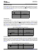
Table 10. Default Mapping
PIN PxMAPy MNEMONIC INPUT PIN FUNCTION OUTPUT PIN FUNCTION
USCI_B1 SPI slave transmit enable (direction controlled by USCI)
P4.0/P4MAP0 PM_UCB1STE/PM_UCA1CLK
USCI_A1 clock input/output (direction controlled by USCI)
USCI_B1 SPI slave in master out (direction controlled by USCI)
P4.1/P4MAP1 PM_UCB1SIMO/PM_UCB1SDA
USCI_B1 I2C data (open drain and direction controlled by USCI)
USCI_B1 SPI slave out master in (direction controlled by USCI)
P4.2/P4MAP2 PM_UCB1SOMI/PM_UCB1SCL
USCI_B1 I2C clock (open drain and direction controlled by USCI)
USCI_A1 SPI slave transmit enable (direction controlled by USCI)
P4.3/P4MAP3 PM_UCB1CLK/PM_UCA1STE
USCI_B1 clock input/output (direction controlled by USCI)
USCI_A1 UART TXD (Direction controlled by USCI - output)
P4.4/P4MAP4 PM_UCA1TXD/PM_UCA1SIMO
USCI_A1 SPI slave in master out (direction controlled by USCI)
USCI_A1 UART RXD (Direction controlled by USCI - input)
P4.5/P4MAP5 PM_UCA1RXD/PM_UCA1SOMI
USCI_A1 SPI slave out master in (direction controlled by USCI)
P4.6/P4MAP6 PM_NONE None DVSS
P4.7/P4MAP7 PM_NONE None DVSS
Oscillator and System Clock (Link to User's Guide)
The clock system in the MSP430F532x family of devices is supported by the Unified Clock System (UCS)
module that includes support for a 32-kHz watch crystal oscillator (XT1 LF mode only; XT1 HF mode is not
supported), an internal very-low-power low-frequency oscillator (VLO), an internal trimmed low-frequency
oscillator (REFO), an integrated internal digitally-controlled oscillator (DCO), and a high-frequency crystal
oscillator XT2. The UCS module is designed to meet the requirements of both low system cost and low power
consumption. The UCS module features digital frequency-locked loop (FLL) hardware that, in conjunction with a
digital modulator, stabilizes the DCO frequency to a programmable multiple of the selected FLL reference
frequency. The internal DCO provides a fast turn-on clock source and stabilizes in 3.5 µs (typical). The UCS
module provides the following clock signals:
• Auxiliary clock (ACLK), sourced from a 32-kHz watch crystal (XT1), a high-frequency crystal (XT2), the
internal low-frequency oscillator (VLO), the trimmed low-frequency oscillator (REFO), or the internal DCO.
• Main clock (MCLK), the system clock used by the CPU. MCLK can be sourced by same sources made
available to ACLK.
• Sub-Main clock (SMCLK), the subsystem clock used by the peripheral modules. SMCLK can be sourced by
same sources made available to ACLK.
• ACLK/n, the buffered output of ACLK, ACLK/2, ACLK/4, ACLK/8, ACLK/16, ACLK/32.
Power Management Module (PMM) (Link to User's Guide)
The PMM includes an integrated voltage regulator that supplies the core voltage to the device and contains
programmable output levels to provide for power optimization. The PMM also includes supply voltage supervisor
(SVS) and supply voltage monitoring (SVM) circuitry, as well as brownout protection. The brownout circuit is
implemented to provide the proper internal reset signal to the device during power-on and power-off. The
SVS/SVM circuitry detects if the supply voltage drops below a user-selectable level and supports both supply
voltage supervision (the device is automatically reset) and supply voltage monitoring (the device is not
automatically reset). SVS and SVM circuitry are available on the primary supply and core supply.
Hardware Multiplier (MPY) (Link to User's Guide)
The multiplication operation is supported by a dedicated peripheral module. The module performs operations with
32-bit, 24-bit, 16-bit, and 8-bit operands. The module is capable of supporting signed and unsigned multiplication
as well as signed and unsigned multiply and accumulate operations.
Real-Time Clock (RTC_A) (Link to User's Guide)
The RTC_A module can be used as a general-purpose 32-bit counter (counter mode) or as an integrated real-
time clock (RTC) (calendar mode). In counter mode, the RTC_A also includes two independent 8-bit timers that
can be cascaded to form a 16-bit timer/counter. Both timers can be read and written by software. Calendar mode
integrates an internal calendar which compensates for months with less than 31 days and includes leap year
correction. The RTC_A also supports flexible alarm functions and offset-calibration hardware.
20 Submit Documentation Feedback Copyright © 2010–2013, Texas Instruments Incorporated