
Datasheet


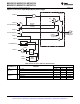


P3.2/PM_TD0_0/PM_SMCLK/CB14
P3.3/PM_TA0CLK/PM_CBOUT/CB13
Direction
0: Input
1: Output
P3SEL.x
1
0
P3DIR.x
P3IN.x
EN
To Port Mapping
1
0
From Port Mapping
P3OUT.x
1
0
DV
SS
DV
CC
P3REN.x
1
P3DS.x
0: Low drive
1: High drive
D
Pad Logic
To Comparator_B
From Comparator_B
CBPD.y
P3MAP.x = PMAP_ANALOG
From Port Mapping
Bus
Holder
MSP430F5172, MSP430F5152, MSP430F5132
MSP430F5171, MSP430F5151, MSP430F5131
SLAS619K –AUGUST 2010–REVISED JANUARY 2014
www.ti.com
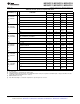
Port P3, P3.2 and P3.3, Input/Output With Schmitt Trigger
Table 50. Port P3 (P3.2 and P3.3) Pin Functions
CONTROL BITS/SIGNALS
(1)
PIN NAME (P3.x) x FUNCTION
P3DIR.x P3SEL.x P3MAP.x CBPD.y
P3.2/ 2 P3.x (I/O) I: 0; O: 1 0 X 0
PM_TD0.0/ TD0.CCI0A 0 1 default 0
PM_SMCLK/ SMCLK output 1 1 default 0
CB14 CB14 X X X 1 (y = 14)
P3.3/ 3 P3.x (I/O) I: 0; O: 1 0 X 0
PM_TA0CLK/ TA0.TA0CLK 0 1 default 0
PM_CBOUT/ CBOUT 1 1 default 0
CB13 CB13 X X X 1 (y = 13)
(1) X = Don't care
78 Submit Documentation Feedback Copyright © 2010–2014, Texas Instruments Incorporated
Product Folder Links: MSP430F5172 MSP430F5152 MSP430F5132 MSP430F5171 MSP430F5151 MSP430F5131