
Datasheet


MSP430F47x
MIXED SIGNAL MICROCONTROLLER
SLAS629A -- MARCH 2009 -- REVISED APRIL 2009
72
POST OFFICE BOX 655303 • DALLAS, TEXAS 75265
APPLICATION INFORMATION
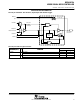
Port P3 pin schematic: P3.1 and P3.2, input/output with Schmitt trigger
Direction
0: Input
1: Output
P3SEL.x
P3DIR.x
P3IN.x
D
EN
Module X IN
Module X OUT
P3OUT.x
Pad Logic
1
0
1
0
P3.1/UCB0SIMO/UCB0SDA/S26
P3.2/UCB0SOMI/UCB0SCL/S27
Module
direction
Segment Sy
LCDS24
Bus
Keeper
EN
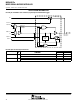
Port P3 (P3.1 and P3.2) pin functions
P
I
N
N
A
M
E
(
P
3
X
)
X
F
U
N
C
T
I
O
N
CONTROL BITS / SIGNALS
PIN N
A
ME
(
P3.
X
)
X
FUNCTION
P3DIR.x P3SEL.x LCDS24
P3.1/UCB0SIMO/ 1 P3.x (I/O) I: 0, O: 1 0 0
/
/
UCB0SDA/S26
UCB0SIMO/UCB0SDA (see Notes 2 and 3) x 1 0
S26 x x 1
P3.2/UCB00SOMI/ 2 P3.x (I/O) I: 0, O: 1 0 0
/
/
UCB0SCL/S27
UCB0SOMI/UCB0SCL (see Notes 2 and 3) x 1 0
S27 x x 1
NOTES: 1. x: Don’t care
2. The pin direction is controlled by the USCI module.
3. In case the I2C functionality is selected the output drives only the logical 0 to V
SS
level.