
Datasheet


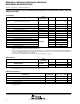


Table Of Contents
- features
- description
- DEVELOPMENT TOOL SUPPORT
- pin designation, MSP430x4351IPN, MSP430x4361IPN, MSP430x4371IPN
- pin designation, MSP430x435IPZ, MSP430x436IPZ, MSP430x4371IPZ
- pin designation, MSP430x435IPN, MSP430x436IPN, MSP430x437IPN
- pin designation, MSP430x435IPZ, MSP430x436IPZ, MSP430x437IPZ
- pin designation, MSP430x4481IPZ, MSP430x4491IPZ
- pin designation, MSP430x447IPZ, MSP430x448IPZ, MSP430x449IPZ
- MSP430x43x1 functional block diagram
- MSP430x43x functional block diagram
- MSP430x44x1 functional block diagram
- MSP430x44x functional block diagram
- MSP430x43x1 Terminal Functions
- MSP430x43x Terminal Functions
- MSP430x44x1 Terminal Functions
- MSP430x44x Terminal Functions
- short-form description
- CPU
- instruction set
- operating modes
- interrupt vector addresses
- special function registers
- interrupt enable 1 and 2
- interrupt flag register 1 and 2
- module enable registers 1 and 2
- memory organization
- bootstrap loader (BSL)
- flash memory
- peripherals
- digital I/O
- oscillator and system clock
- brownout, supply voltage supervisor (SVS)
- hardware multiplier (MSP430x44x(1) only)
- watchdog timer (WDT)
- USART0
- USART1 (MSP430x44x(1) only)
- Timer_A3
- Timer_B3 (MSP430x43x(1) only)
- Timer_B7 (MSP430x44x(1) only)
- Comparator_A
- ADC12 (not implemented in MSP430x43x1 and MSP430x44x1)
- Basic Timer1
- LCD driver
- peripheral file map
- absolute maximum ratings
- recommended operating conditions
- electrical characteristics
- supply current into AVCC + DVCC excluding external current
- Schmitt-trigger inputs - ports P1, P2, P3, P4, P5, P6
- standard inputs - RST/NMI, JTAG (TCK, TMS, TDI/TCLK)
- inputs Px.x, TAx, TBx
- leakage current
- outputs - ports P1, P2, P3, P4, P5, P6
- output frequency
- wake-up LPM3
- RAM
- LCD
- Comparator_A
- POR/brownout reset (BOR)
- supply voltage supervisor/monitor (SVS)
- DCO
- crystal oscillator, LFXT1 oscillator
- crystal oscillator, XT2 oscillator
- USART0, USART1
- 12-bit ADC, power supply and input range conditions
- 12-bit ADC, external reference
- 12-bit ADC, built-in reference
- 12-bit ADC, timing parameters
- 12-bit ADC, linearity parameters
- 12-bit ADC, temperature sensor and built-in VMID
- flash memory
- JTAG interface
- JTAG fuse
- APPLICATION INFORMATION
- input/output schematics
- port P1, P1.0 to P1.5, input/output with Schmitt trigger
- port P1, P1.6, P1.7, input/output with Schmitt trigger
- port P2, P2.0, P2.4 to P2.5, input/output with Schmitt trigger
- port P2, P2.1 to P2.3, input/output with Schmitt trigger
- port P2, P2.6 to P2.7, input/output with Schmitt trigger
- port P3, P3.0 to P3.3, input/output with Schmitt trigger
- port P3, P3.4 to P3.7, input/output with Schmitt trigger
- port P4, P4.0 to P4.7, input/output with Schmitt trigger
- port P5, P5.0 to P5.1, input/output with Schmitt trigger
- port P5, P5.2 to P5.4, input/output with Schmitt trigger
- port P5, P5.5 to P5.7, input/output with Schmitt trigger
- port P6, P6.0 to P6.6, input/output with Schmitt trigger
- port P6, P6.0 to P6.6, input/output with Schmitt trigger
- port P6, P6.7, input/output with Schmitt trigger
- JTAG pins TMS, TCK, TDI/TCLK, TDO/TDI, input/output with Schmitt trigger or output
- JTAG fuse check mode
- input/output schematics
- Data Sheet Revision History

MSP430x43x1, MSP430x43x, MSP430x44x1, MSP430x44x
MIXED SIGNAL MICROCONTROLLER
SLAS344G − JANUARY 2002 − REVISED OCTOBER 2009
54
POST OFFICE BOX 655303 • DALLAS, TEXAS 75265
electrical characteristics over recommended operating free-air temperature (unless otherwise
noted) (continued)
12-bit ADC, timing parameters
PARAMETER TEST CONDITIONS V
CC
MIN TYP MAX UNIT
f
ADC12CLK
For specified performance of ADC12
linearity parameters
2.2V/3 V 0.45 5 6.3 MHz
f
ADC12OSC
Internal ADC12
oscillator
ADC12DIV=0,
f
ADC12CLK
=f
ADC12OSC
2.2 V/ 3 V 3.7 6.3 MHz
t
Conversion time
C
VREF+
≥ 5 µF, Internal oscillator,
f
ADC12OSC
= 3.7 MHz to 6.3 MHz
2.2 V/ 3 V 2.06 3.51 µs
t
CONVERT
Conversion time
External f
ADC12CLK
from ACLK, MCLK
or SMCLK: ADC12SSEL ≠ 0
13×ADC12DIV×
1/f
ADC12CLK
µs
t
ADC12ON
Turn on settling time of
the ADC
See Note 1 100 ns
t
Sampling time
R
S
= 400 Ω, R
I
= 1000 Ω,
C 30 pF
3 V 1220
ns
t
Sample
Sampling time
C
I
= 30 pF
τ = [R
S
+ R
I
] x C
I;
(see Note 2)
2.2 V 1400
ns
NOTES: 1. The condition is that the error in a conversion started after t
ADC12ON
is less than ±0.5 LSB. The reference and input signal are already
settled.
2. Approximately ten Tau (τ) are needed to get an error of less than ±0.5 LSB:
t
Sample
= ln(2
n+1
) x (R
S
+ R
I
) x C
I
+ 800 ns where n = ADC resolution = 12, R
S
= external source resistance.
12-bit ADC, linearity parameters
PARAMETER TEST CONDITIONS V
CC
MIN TYP MAX UNIT
E
Integral linearity error
1.4 V ≤ (V
eREF+
− V
REF−
/V
eREF−
) min ≤ 1.6 V
2 2 V/3 V
±2
LSB
E
I
Integral linearity error
1.6 V < (V
eREF+
− V
REF−
/V
eREF−
) min ≤ [V
(AVCC)
]
2.2 V/3 V
±1.7
LSB
E
D
Differential linearity
error
(V
eREF+
− V
REF−
/V
eREF−
)
min
≤ (V
eREF+
− V
REF−
/V
eREF−
),
C
VREF+
= 10 µF (tantalum) and 100 nF (ceramic)
2.2 V/3 V ±1 LSB
E
O
Offset error
(V
eREF+
− V
REF−
/V
eREF−
)
min
≤ (V
eREF+
− V
REF−
/V
eREF−
),
Internal impedance of source R
S
< 100 Ω,
C
VREF+
= 10 µF (tantalum) and 100 nF (ceramic)
2.2 V/3 V ±2 ±4 LSB
E
G
Gain error
(V
eREF+
− V
REF−
/V
eREF−
)
min
≤ (V
eREF+
− V
REF−
/V
eREF−
),
C
VREF+
= 10 µF (tantalum) and 100 nF (ceramic)
2.2 V/3 V ±1.1 ±2 LSB
E
T
Total unadjusted
error
(V
eREF+
− V
REF−
/V
eREF−
)
min
≤ (V
eREF+
− V
REF−
/V
eREF−
),
C
VREF+
= 10 µF (tantalum) and 100 nF (ceramic)
2.2 V/3 V ±2 ±5 LSB