
Datasheet


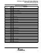


Table Of Contents
- features
- description
- DEVELOPMENT TOOL SUPPORT
- pin designation, MSP430x4351IPN, MSP430x4361IPN, MSP430x4371IPN
- pin designation, MSP430x435IPZ, MSP430x436IPZ, MSP430x4371IPZ
- pin designation, MSP430x435IPN, MSP430x436IPN, MSP430x437IPN
- pin designation, MSP430x435IPZ, MSP430x436IPZ, MSP430x437IPZ
- pin designation, MSP430x4481IPZ, MSP430x4491IPZ
- pin designation, MSP430x447IPZ, MSP430x448IPZ, MSP430x449IPZ
- MSP430x43x1 functional block diagram
- MSP430x43x functional block diagram
- MSP430x44x1 functional block diagram
- MSP430x44x functional block diagram
- MSP430x43x1 Terminal Functions
- MSP430x43x Terminal Functions
- MSP430x44x1 Terminal Functions
- MSP430x44x Terminal Functions
- short-form description
- CPU
- instruction set
- operating modes
- interrupt vector addresses
- special function registers
- interrupt enable 1 and 2
- interrupt flag register 1 and 2
- module enable registers 1 and 2
- memory organization
- bootstrap loader (BSL)
- flash memory
- peripherals
- digital I/O
- oscillator and system clock
- brownout, supply voltage supervisor (SVS)
- hardware multiplier (MSP430x44x(1) only)
- watchdog timer (WDT)
- USART0
- USART1 (MSP430x44x(1) only)
- Timer_A3
- Timer_B3 (MSP430x43x(1) only)
- Timer_B7 (MSP430x44x(1) only)
- Comparator_A
- ADC12 (not implemented in MSP430x43x1 and MSP430x44x1)
- Basic Timer1
- LCD driver
- peripheral file map
- absolute maximum ratings
- recommended operating conditions
- electrical characteristics
- supply current into AVCC + DVCC excluding external current
- Schmitt-trigger inputs - ports P1, P2, P3, P4, P5, P6
- standard inputs - RST/NMI, JTAG (TCK, TMS, TDI/TCLK)
- inputs Px.x, TAx, TBx
- leakage current
- outputs - ports P1, P2, P3, P4, P5, P6
- output frequency
- wake-up LPM3
- RAM
- LCD
- Comparator_A
- POR/brownout reset (BOR)
- supply voltage supervisor/monitor (SVS)
- DCO
- crystal oscillator, LFXT1 oscillator
- crystal oscillator, XT2 oscillator
- USART0, USART1
- 12-bit ADC, power supply and input range conditions
- 12-bit ADC, external reference
- 12-bit ADC, built-in reference
- 12-bit ADC, timing parameters
- 12-bit ADC, linearity parameters
- 12-bit ADC, temperature sensor and built-in VMID
- flash memory
- JTAG interface
- JTAG fuse
- APPLICATION INFORMATION
- input/output schematics
- port P1, P1.0 to P1.5, input/output with Schmitt trigger
- port P1, P1.6, P1.7, input/output with Schmitt trigger
- port P2, P2.0, P2.4 to P2.5, input/output with Schmitt trigger
- port P2, P2.1 to P2.3, input/output with Schmitt trigger
- port P2, P2.6 to P2.7, input/output with Schmitt trigger
- port P3, P3.0 to P3.3, input/output with Schmitt trigger
- port P3, P3.4 to P3.7, input/output with Schmitt trigger
- port P4, P4.0 to P4.7, input/output with Schmitt trigger
- port P5, P5.0 to P5.1, input/output with Schmitt trigger
- port P5, P5.2 to P5.4, input/output with Schmitt trigger
- port P5, P5.5 to P5.7, input/output with Schmitt trigger
- port P6, P6.0 to P6.6, input/output with Schmitt trigger
- port P6, P6.0 to P6.6, input/output with Schmitt trigger
- port P6, P6.7, input/output with Schmitt trigger
- JTAG pins TMS, TCK, TDI/TCLK, TDO/TDI, input/output with Schmitt trigger or output
- JTAG fuse check mode
- input/output schematics
- Data Sheet Revision History

MSP430x43x1, MSP430x43x, MSP430x44x1, MSP430x44x
MIXED SIGNAL MICROCONTROLLER
SLAS344G − JANUARY 2002 − REVISED OCTOBER 2009
20
POST OFFICE BOX 655303 • DALLAS, TEXAS 75265
MSP430x44x Terminal Functions
TERMINAL
I/O
DESCRIPTION
NAME NO.
I/O
DESCRIPTION
DV
CC1
1 Digital supply voltage, positive terminal.
P6.3/A3 2 I/O General-purpose digital I/O / analog input a3—12-bit ADC
P6.4/A4 3 I/O General-purpose digital I/O / analog input a4—12-bit ADC
P6.5/A5 4 I/O General-purpose digital I/O / analog input a5—12-bit ADC
P6.6/A6 5 I/O General-purpose digital I/O / analog input a6—12-bit ADC
P6.7/A7/SVSIN 6 I/O
General-purpose digital I/O / analog input a7—12-bit ADC / analog input to brownout, supply voltage
supervisor
V
REF+
7 O Output of positive terminal of the reference voltage in the ADC
XIN 8 I Input port for crystal oscillator XT1. Standard or watch crystals can be connected.
XOUT 9 O Output terminal of crystal oscillator XT1
Ve
REF+
10 I Input for an external reference voltage to the ADC
V
REF−
/Ve
REF−
11 I
Negative terminal for the ADC’s reference voltage for both sources, the internal reference voltage, or an
external applied reference voltage
P5.1/S0 12 I/O General-purpose digital I/O / LCD segment output 0
P5.0/S1 13 I/O General-purpose digital I/O / LCD segment output 1
S2 14 O LCD segment output 2
S3 15 O LCD segment output 3
S4 16 O LCD segment output 4
S5 17 O LCD segment output 5
S6 18 O LCD segment output 6
S7 19 O LCD segment output 7
S8 20 O LCD segment output 8
S9 21 O LCD segment output 9
S10 22 O LCD segment output 10
S11 23 O LCD segment output 11
S12 24 O LCD segment output 12
S13 25 O LCD segment output 13
S14 26 O LCD segment output 14
S15 27 O LCD segment output 15
S16 28 O LCD segment output 16
S17 29 O LCD segment output 17
S18 30 O LCD segment output 18
S19 31 O LCD segment output 19
S20 32 O LCD segment output 20
S21 33 O LCD segment output 21
S22 34 O LCD segment output 22
S23 35 O LCD segment output 23
S24 36 O LCD segment output 24
S25 37 O LCD segment output 25
S26 38 O LCD segment output 26
S27 39 O LCD segment output 27
S28 40 O LCD segment output 28