
Datasheet


MSP430x43x1, MSP430x43x, MSP430x44x1, MSP430x44x
MIXED SIGNAL MICROCONTROLLER
SLAS344G − JANUARY 2002 − REVISED OCTOBER 2009
56
POST OFFICE BOX 655303 • DALLAS, TEXAS 75265
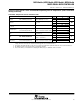
electrical characteristics over recommended operating free-air temperature (unless otherwise
noted) (continued)
flash memory
PARAMETER
TEST
CONDITIONS
V
CC
MIN TYP MAX UNIT
V
CC(PGM/
ERASE)
Program and Erase supply voltage 2.7 3.6 V
f
FTG
Flash Timing Generator frequency 257 476 kHz
I
PGM
Supply current from DV
CC
during program 2.7 V/ 3.6 V 3 5 mA
I
ERASE
Supply current from DV
CC
during erase 2.7 V/ 3.6 V 3 7 mA
t
CPT
Cumulative program time See Note 1 2.7 V/ 3.6 V 10 ms
t
CMErase
Cumulative mass erase time See Note 2 2.7 V/ 3.6 V 200 ms
Program/Erase endurance 10
4
10
5
cycles
t
Retention
Data retention duration T
J
= 25°C 100 years
t
Word
Word or byte program time 35
t
Block,
0
Block program time for 1
st
byte or word 30
t
Block,
1-63
Block program time for each additional byte or word
see Note 3
21
t
t
Block,
End
Block program end-sequence wait time
see Note 3
6
t
FTG
t
Mass
Erase
Mass erase time 5297
t
Seg
Erase
Segment erase time 4819
NOTES: 1. The cumulative program time must not be exceeded when writing to a 64-byte flash block. This parameter applies to all programming
methods: individual word/byte write and block write modes.
2. The mass erase duration generated by the flash timing generator is at least 11.1ms ( = 5297x1/f
FTG
,max = 5297x1/476kHz). To
achieve the required cumulative mass erase time the Flash Controller’s mass erase operation can be repeated until this time is met.
(A worst case minimum of 19 cycles are required).
3. These values are hardwired into the Flash Controller’s state machine (t
FTG
= 1/f
FTG
).
JTAG interface
PARAMETER
TEST
CONDITIONS
V
CC
MIN TYP MAX UNIT
f
TCK input frequency
see Note 1
2.2 V 0 5 MHz
f
TCK
TCK input frequency see Note 1
3 V 0 10 MHz
R
Internal
Internal pullup resistance on TMS, TCK, TDI/TCLK see Note 2 2.2 V/ 3 V 25 60 90 kΩ
NOTES: 1. f
TCK
may be restricted to meet the timing requirements of the module selected.
2. TMS, TDI/TCLK, and TCK pull-up resistors are implemented in all versions.
JTAG fuse (see Note 1)
PARAMETER
TEST
CONDITIONS
MIN TYP MAX UNIT
V
CC(FB)
Supply voltage during fuse-blow condition T
A
= 25°C 2.5 V
V
FB
Voltage level on TDI/TCLK for fuse-blow: F versions 6 7 V
I
FB
Supply current into TDI/TCLK during fuse blow 100 mA
t
FB
Time to blow fuse 1 ms
NOTES: 1. Once the fuse is blown, no further access to the MSP430 JTAG/Test and emulation features is possible. The JTAG block is switched
to bypass mode.