
Datasheet


MSP430x43x1, MSP430x43x, MSP430x44x1, MSP430x44x
MIXED SIGNAL MICROCONTROLLER
SLAS344G − JANUARY 2002 − REVISED OCTOBER 2009
50
POST OFFICE BOX 655303 • DALLAS, TEXAS 75265
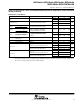
electrical characteristics over recommended operating free-air temperature (unless otherwise
noted) (continued)
crystal oscillator, LFXT1 oscillator (see Notes 1 and 2)
PARAMETER TEST CONDITIONS V
CC
MIN TYP MAX UNIT
OSCCAPx = 0h
2.2 V / 3 V
0
C
XIN
Inte
g
rated in
p
ut ca
p
acitance
OSCCAPx = 1h
2.2 V/3 V 10
p
F
C
XIN
Integrated
input
capacitance
OSCCAPx = 2h 2.2 V/3 V 14
pF
OSCCAPx = 3h 2.2 V/3 V 18
OSCCAPx = 0h 2.2 V/3 V 0
C
Integrated output capacitance
OSCCAPx = 1h 2.2 V/3 V 10
pF
C
XOUT
Integrated output capacitance
OSCCAPx = 2h
2.2 V/3 V 14
pF
OSCCAPx = 3h 2.2 V/3 V 18
V
IL
Input levels at XIN
See Note 3
2 2 V/3 V
V
SS
0.2 × V
CC
V
V
IH
Input levels at XIN See Note 3 2.2 V/3 V
0.8 × V
CC
V
CC
V
NOTES: 1. The parasitic capacitance from the package and board may be estimated to be 2 pF. The effective load capacitor for the crystal is
(C
XIN
xC
XOUT
) / (C
XIN
+ C
XOUT
). This is independent of XTS_FLL.
2. To improve EMI on the low-power LFXT1 oscillator, particularly in the LF mode (32 kHz), the following guidelines should be observed.
− Keep the trace between the ’F43x(1)/44x(1) and the crystal as short as possible.
− Design a good ground plane around the oscillator pins.
− Prevent crosstalk from other clock or data lines into oscillator pins XIN and XOUT.
− Avoid running PCB traces underneath or adjacent to the XIN and XOUT pins.
− Use assembly materials and praxis to avoid any parasitic load on the oscillator XIN and XOUT pins.
− If conformal coating is used, ensure that it does not induce capacitive/resistive leakage between the oscillator pins.
− Do not route the XOUT line to the JTAG header to support the serial programming adapter as shown in other
documentation. This signal is no longer required for the serial programming adapter.
3. Applies only when using an external logic-level clock source. XTS_FLL must be set. Not applicable when using a crystal or resonator.
4. External capacitance is recommended for precision real-time clock applications; OSCCAPx = 0h.
crystal oscillator, XT2 oscillator (see Note 1)
PARAMETER TEST CONDITIONS MIN NOM MAX UNIT
C
XT2IN
Integrated input capacitance V
CC
= 2.2 V/3 V 2 pF
C
XT2OUT
Integrated output capacitance V
CC
= 2.2 V/3 V 2 pF
V
IL
Input levels at XT2IN
V = 2 2 V/3 V (see Note 2)
V
SS
0.2 × V
CC
V
V
IH
Input levels at XT2IN V
CC
= 2.2 V/3 V (see Note 2)
0.8 × V
CC
V
CC
V
NOTES: 1. The oscillator needs capacitors at both terminals, with values specified by the crystal manufacturer.
2. Applies only when using an external logic-level clock source. Not applicable when using a crystal or resonator.
USART0, USART1 (see Note 1)
PARAMETER TEST CONDITIONS MIN NOM MAX UNIT
t
USART0/1: deglitch time
V
CC
= 2.2 V, SYNC = 0, UART mode 200 430 800
ns
t
(
τ
)
USART0/1: deglitch time
V
CC
= 3 V, SYNC = 0, UART mode 150 280 500
ns
NOTE 1: The signal applied to the USART0/1 receive signal/terminal (URXD0/1) should meet the timing requirements of t
(τ
)
to ensure that the
URXS flip-flop is set. The URXS flip-flop is set with negative pulses meeting the minimum-timing condition of t
(τ
)
. The operating
conditions to set the flag must be met independently from this timing constraint. The deglitch circuitry is active only on negative
transitions on the URXD0/1 line.