
Datasheet


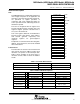


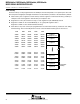


Table Of Contents
- features
- description
- DEVELOPMENT TOOL SUPPORT
- pin designation, MSP430x4351IPN, MSP430x4361IPN, MSP430x4371IPN
- pin designation, MSP430x435IPZ, MSP430x436IPZ, MSP430x4371IPZ
- pin designation, MSP430x435IPN, MSP430x436IPN, MSP430x437IPN
- pin designation, MSP430x435IPZ, MSP430x436IPZ, MSP430x437IPZ
- pin designation, MSP430x4481IPZ, MSP430x4491IPZ
- pin designation, MSP430x447IPZ, MSP430x448IPZ, MSP430x449IPZ
- MSP430x43x1 functional block diagram
- MSP430x43x functional block diagram
- MSP430x44x1 functional block diagram
- MSP430x44x functional block diagram
- MSP430x43x1 Terminal Functions
- MSP430x43x Terminal Functions
- MSP430x44x1 Terminal Functions
- MSP430x44x Terminal Functions
- short-form description
- CPU
- instruction set
- operating modes
- interrupt vector addresses
- special function registers
- interrupt enable 1 and 2
- interrupt flag register 1 and 2
- module enable registers 1 and 2
- memory organization
- bootstrap loader (BSL)
- flash memory
- peripherals
- digital I/O
- oscillator and system clock
- brownout, supply voltage supervisor (SVS)
- hardware multiplier (MSP430x44x(1) only)
- watchdog timer (WDT)
- USART0
- USART1 (MSP430x44x(1) only)
- Timer_A3
- Timer_B3 (MSP430x43x(1) only)
- Timer_B7 (MSP430x44x(1) only)
- Comparator_A
- ADC12 (not implemented in MSP430x43x1 and MSP430x44x1)
- Basic Timer1
- LCD driver
- peripheral file map
- absolute maximum ratings
- recommended operating conditions
- electrical characteristics
- supply current into AVCC + DVCC excluding external current
- Schmitt-trigger inputs - ports P1, P2, P3, P4, P5, P6
- standard inputs - RST/NMI, JTAG (TCK, TMS, TDI/TCLK)
- inputs Px.x, TAx, TBx
- leakage current
- outputs - ports P1, P2, P3, P4, P5, P6
- output frequency
- wake-up LPM3
- RAM
- LCD
- Comparator_A
- POR/brownout reset (BOR)
- supply voltage supervisor/monitor (SVS)
- DCO
- crystal oscillator, LFXT1 oscillator
- crystal oscillator, XT2 oscillator
- USART0, USART1
- 12-bit ADC, power supply and input range conditions
- 12-bit ADC, external reference
- 12-bit ADC, built-in reference
- 12-bit ADC, timing parameters
- 12-bit ADC, linearity parameters
- 12-bit ADC, temperature sensor and built-in VMID
- flash memory
- JTAG interface
- JTAG fuse
- APPLICATION INFORMATION
- input/output schematics
- port P1, P1.0 to P1.5, input/output with Schmitt trigger
- port P1, P1.6, P1.7, input/output with Schmitt trigger
- port P2, P2.0, P2.4 to P2.5, input/output with Schmitt trigger
- port P2, P2.1 to P2.3, input/output with Schmitt trigger
- port P2, P2.6 to P2.7, input/output with Schmitt trigger
- port P3, P3.0 to P3.3, input/output with Schmitt trigger
- port P3, P3.4 to P3.7, input/output with Schmitt trigger
- port P4, P4.0 to P4.7, input/output with Schmitt trigger
- port P5, P5.0 to P5.1, input/output with Schmitt trigger
- port P5, P5.2 to P5.4, input/output with Schmitt trigger
- port P5, P5.5 to P5.7, input/output with Schmitt trigger
- port P6, P6.0 to P6.6, input/output with Schmitt trigger
- port P6, P6.0 to P6.6, input/output with Schmitt trigger
- port P6, P6.7, input/output with Schmitt trigger
- JTAG pins TMS, TCK, TDI/TCLK, TDO/TDI, input/output with Schmitt trigger or output
- JTAG fuse check mode
- input/output schematics
- Data Sheet Revision History

MSP430x43x1, MSP430x43x, MSP430x44x1, MSP430x44x
MIXED SIGNAL MICROCONTROLLER
SLAS344G − JANUARY 2002 − REVISED OCTOBER 2009
29
POST OFFICE BOX 655303 • DALLAS, TEXAS 75265
peripherals
Peripherals are connected to the CPU through data, address, and control buses and can be handled using all
instructions. For complete module descriptions, see the MSP430x4xx Family User’s Guide, literature number
SLAU056.
digital I/O
There are six 8-bit I/O ports implemented—ports P1 through P6:
D All individual I/O bits are independently programmable.
D Any combination of input, output, and interrupt conditions is possible.
D Edge-selectable interrupt input capability for all the eight bits of ports P1 and P2.
D Read/write access to port-control registers is supported by all instructions.
oscillator and system clock
The clock system in the MSP430x43x(1) and MSP43x44x(1) family of devices is supported by the FLL+ module,
which includes support for a 32768-Hz watch crystal oscillator, an internal digitally controlled oscillator (DCO),
and a high-frequency crystal oscillator. The FLL+ clock module is designed to meet the requirements of both
low system cost and low power consumption. The FLL+ features a digital frequency-locked loop (FLL) hardware
that, in conjunction with a digital modulator, stabilizes the DCO frequency to a programmable multiple of the
watch crystal frequency. The internal DCO provides a fast turn-on clock source and stabilizes in less than 6 µs.
The FLL+ module provides the following clock signals:
D Auxiliary clock (ACLK), sourced from a 32768-Hz watch crystal or a high-frequency crystal
D Main clock (MCLK), the system clock used by the CPU
D Sub-Main clock (SMCLK), the sub-system clock used by the peripheral modules
D ACLK/n, the buffered output of ACLK, ACLK/2, ACLK/4, or ACLK/8
brownout, supply voltage supervisor (SVS)
The brownout circuit is implemented to provide the proper internal reset signal to the device during power on
and power off. The supply voltage supervisor (SVS) circuitry detects if the supply voltage drops below a user
selectable level and supports both supply voltage supervision (the device is automatically reset) and supply
voltage monitoring (SVM, the device is not automatically reset).
The CPU begins code execution after the brownout circuit releases the device reset. However, V
CC
may not
have ramped to V
CC(min)
at that time. The user must insure the default FLL+ settings are not changed until V
CC
reaches V
CC(min)
. If desired, the SVS circuit can be used to determine when V
CC
reaches V
CC(min)
.
hardware multiplier (MSP430x44x(1) only)
The multiplication operation is supported by a dedicated peripheral module. The module performs 16 16,
16 8, 8 16, and 8 8 bit operations. The module is capable of supporting signed and unsigned multiplication
as well as signed and unsigned multiply and accumulate operations. The result of an operation can be accessed
immediately after the operands have been loaded into the peripheral registers. No additional clock cycles are
required.
watchdog timer (WDT)
The primary function of the watchdog timer (WDT) module is to perform a controlled system restart after a
software problem occurs. If the selected time interval expires, a system reset is generated. If the watchdog
function is not needed in an application, the module can be configured as an interval timer and can generate
interrupts at selected time intervals.