
Datasheet


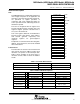


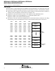


Table Of Contents
- features
- description
- DEVELOPMENT TOOL SUPPORT
- pin designation, MSP430x4351IPN, MSP430x4361IPN, MSP430x4371IPN
- pin designation, MSP430x435IPZ, MSP430x436IPZ, MSP430x4371IPZ
- pin designation, MSP430x435IPN, MSP430x436IPN, MSP430x437IPN
- pin designation, MSP430x435IPZ, MSP430x436IPZ, MSP430x437IPZ
- pin designation, MSP430x4481IPZ, MSP430x4491IPZ
- pin designation, MSP430x447IPZ, MSP430x448IPZ, MSP430x449IPZ
- MSP430x43x1 functional block diagram
- MSP430x43x functional block diagram
- MSP430x44x1 functional block diagram
- MSP430x44x functional block diagram
- MSP430x43x1 Terminal Functions
- MSP430x43x Terminal Functions
- MSP430x44x1 Terminal Functions
- MSP430x44x Terminal Functions
- short-form description
- CPU
- instruction set
- operating modes
- interrupt vector addresses
- special function registers
- interrupt enable 1 and 2
- interrupt flag register 1 and 2
- module enable registers 1 and 2
- memory organization
- bootstrap loader (BSL)
- flash memory
- peripherals
- digital I/O
- oscillator and system clock
- brownout, supply voltage supervisor (SVS)
- hardware multiplier (MSP430x44x(1) only)
- watchdog timer (WDT)
- USART0
- USART1 (MSP430x44x(1) only)
- Timer_A3
- Timer_B3 (MSP430x43x(1) only)
- Timer_B7 (MSP430x44x(1) only)
- Comparator_A
- ADC12 (not implemented in MSP430x43x1 and MSP430x44x1)
- Basic Timer1
- LCD driver
- peripheral file map
- absolute maximum ratings
- recommended operating conditions
- electrical characteristics
- supply current into AVCC + DVCC excluding external current
- Schmitt-trigger inputs - ports P1, P2, P3, P4, P5, P6
- standard inputs - RST/NMI, JTAG (TCK, TMS, TDI/TCLK)
- inputs Px.x, TAx, TBx
- leakage current
- outputs - ports P1, P2, P3, P4, P5, P6
- output frequency
- wake-up LPM3
- RAM
- LCD
- Comparator_A
- POR/brownout reset (BOR)
- supply voltage supervisor/monitor (SVS)
- DCO
- crystal oscillator, LFXT1 oscillator
- crystal oscillator, XT2 oscillator
- USART0, USART1
- 12-bit ADC, power supply and input range conditions
- 12-bit ADC, external reference
- 12-bit ADC, built-in reference
- 12-bit ADC, timing parameters
- 12-bit ADC, linearity parameters
- 12-bit ADC, temperature sensor and built-in VMID
- flash memory
- JTAG interface
- JTAG fuse
- APPLICATION INFORMATION
- input/output schematics
- port P1, P1.0 to P1.5, input/output with Schmitt trigger
- port P1, P1.6, P1.7, input/output with Schmitt trigger
- port P2, P2.0, P2.4 to P2.5, input/output with Schmitt trigger
- port P2, P2.1 to P2.3, input/output with Schmitt trigger
- port P2, P2.6 to P2.7, input/output with Schmitt trigger
- port P3, P3.0 to P3.3, input/output with Schmitt trigger
- port P3, P3.4 to P3.7, input/output with Schmitt trigger
- port P4, P4.0 to P4.7, input/output with Schmitt trigger
- port P5, P5.0 to P5.1, input/output with Schmitt trigger
- port P5, P5.2 to P5.4, input/output with Schmitt trigger
- port P5, P5.5 to P5.7, input/output with Schmitt trigger
- port P6, P6.0 to P6.6, input/output with Schmitt trigger
- port P6, P6.0 to P6.6, input/output with Schmitt trigger
- port P6, P6.7, input/output with Schmitt trigger
- JTAG pins TMS, TCK, TDI/TCLK, TDO/TDI, input/output with Schmitt trigger or output
- JTAG fuse check mode
- input/output schematics
- Data Sheet Revision History

MSP430x43x1, MSP430x43x, MSP430x44x1, MSP430x44x
MIXED SIGNAL MICROCONTROLLER
SLAS344G − JANUARY 2002 − REVISED OCTOBER 2009
25
POST OFFICE BOX 655303 • DALLAS, TEXAS 75265
interrupt vector addresses
The interrupt vectors and the power-up starting address are located in the address range 0FFFFh to 0FFE0h.
The vector contains the 16-bit address of the appropriate interrupt-handler instruction sequence.
Table 3. Interrupt Sources, Flags, and Vectors
INTERRUPT SOURCE INTERRUPT FLAG SYSTEM INTERRUPT
WORD
ADDRESS
PRIORITY
Power-Up
External Reset
Watchdog
Flash Memory
WDTIFG
KEYV
(see Note 1)
Reset 0FFFEh 15, highest
NMI
Oscillator Fault
Flash Memory Access Violation
NMIIFG (see Notes 1 and 3)
OFIFG (see Notes 1 and 3)
ACCVIFG (see Notes 1 and 3)
(Non)maskable
(Non)maskable
(Non)maskable
0FFFCh 14
Timer_B7
†
TBCCR0 CCIFG (see Note 2) Maskable 0FFFAh 13
Timer_B7
†
TBCCR1 to TBCCR6 CCIFGs
TBIFG (see Notes 1 and 2)
Maskable 0FFF8h 12
Comparator_A CAIFG Maskable 0FFF6h 11
Watchdog Timer WDTIFG Maskable 0FFF4h 10
USART0 Receive URXIFG0 Maskable 0FFF2h 9
USART0 Transmit UTXIFG0 Maskable 0FFF0h 8
ADC12 (see Note 4) ADC12IFG (see Notes 1 and 2) Maskable 0FFEEh 7
Timer_A3 TACCR0 CCIFG (see Note 2) Maskable 0FFECh 6
Timer_A3
TACCR1 and TACCR2 CCIFGs,
TAIFG (see Notes 1 and 2)
Maskable 0FFEAh 5
I/O Port P1 (Eight Flags)
P1IFG.0 to P1IFG.7
(see Notes 1 and 2)
Maskable 0FFE8h 4
USART1 Receive
‡
URXIFG1 Maskable 0FFE6h 3
USART1 Transmit
‡
UTXIFG1 Maskable 0FFE4h 2
I/O Port P2 (Eight Flags)
P2IFG.0 to P2IFG.7
(see Notes 1 and 2)
Maskable 0FFE2h 1
Basic Timer1 BTIFG Maskable 0FFE0h 0, lowest
†
’43x(1) uses Timer_B3 with TBCCR0, 1 and 2 CCIFG flags, and TBIFG. ’44x(1) uses Timer_B7 with TBCCR0 CCIFG, TBCCR1 to TBCCR6
CCIFGs, and TBIFG
‡
USART1 is implemented in ’44x(1) only.
NOTES: 1. Multiple source flags
2. Interrupt flags are located in the module.
3. (Non)maskable: the individual interrupt-enable bit can disable an interrupt event, but the general-interrupt enable can not disable
it.
4. ADC12 is not implemented in MSP430x43x1 and MSP430x44x1 devices.