
Datasheet


MSP430F42x0
MIXED SIGNAL MICROCONTROLLER
SLAS455D − MARCH 2005 − REVISED APRIL 2007
43
POST OFFICE BOX 655303 • DALLAS, TEXAS 75265
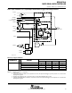
Port P1 pin schematic: P1.4, input/output with Schmitt−trigger and analog functions
Bus
Keeper
EN
Direction
0: Input
1: Output
P1SEL.x
1
0
P1DIR.x
P1IN.x
INCH=3
A3−
Pad Logic
SD16AE.x
Interrupt
Edge
Select
Q
EN
Set
P1SEL.x
P1IES.x
P1IFG.x
P1IE.x
P1IRQ.x
1
0
P1OUT.x
Note: x = 4
P1.4/A3−/DAC0
1
0
AV
SS
DAC12OPS
DAC12OPS
DAC0
DV
SS
’1’ if DAC12AMPx>0
Port P1 (P1.4) pin functions
PIN NAME (P1 X)
X
FUNCTION
CONTROL BITS / SIGNALS
PIN NAME (P1.X)
X FUNCTION
P1DIR.x P1SEL.x SD16AE.x DAC12OPS
P1.4/A3−/DAC0 4
P1.4† Input/Output 0/1 0 0 0
N/A 0 1 0 0
DVSS 1 1 0 0
A3− (see Notes 3, 4) X X 1 0
DAC0 (see Note 5) X X X 1
†
Default after reset (PUC/POR)
NOTES: 1. N/A: Not available or not applicable.
2. X: Don’t care.
3. Setting the SD16AE.x bit disables the output driver as well as the input Schmitt trigger to prevent parasitic cross currents when
applying analog signals.
4. Negative input to SD16_A (A3−) connected to AV
SS
if corresponding SD16AE.x bit is cleared.
5. Setting the DAC12OPS bit also disables the output driver as well as the input Schmitt trigger to prevent parasitic cross currents when
applying analog signals.