
Datasheet


MSP430F42x0
MIXED SIGNAL MICROCONTROLLER
SLAS455D − MARCH 2005 − REVISED APRIL 2007
40
POST OFFICE BOX 655303 • DALLAS, TEXAS 75265
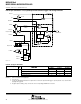
Port P1 pin schematic: P1.2, input/output with Schmitt−trigger and analog functions
Bus
Keeper
EN
Direction
0: Input
1: Output
P1SEL.x
1
0
P1DIR.x
P1IN.x
INCH=4
A4−
Pad Logic
SD16AE.x
P1IRQ.x
D
EN
Module X IN
1
0
Module X OUT
P1OUT.x
Note: x = 2
P1.2/TA1/A4−
1
0
AV
SS
Interrupt
Edge
Select
Q
EN
Set
P1SEL.x
P1IES.x
P1IFG.x
P1IE.x
Port P1 (P1.2) pin functions
PIN NAME (P1 X)
X
FUNCTION
CONTROL BITS / SIGNALS
PIN NAME (P1.X)
X FUNCTION
P1DIR.x P1SEL.x SD16AE.x
P1.2/TA1/A4− 2
P1.2† Input/Output 0/1 0 0
Timer_A3.CCI1A 0 1 0
Timer_A3.TA1 1 1 0
A4− (see Notes 3, 4) X X 1
†
Default after reset (PUC/POR)
NOTES: 1. N/A: Not available or not applicable.
2. X: Don’t care.
3. Setting the SD16AE.x bit disables the output driver as well as the input Schmitt trigger to prevent parasitic cross currents when
applying analog signals.
4. Negative input to SD16_A (A4−) connected to V
SS
if corresponding SD16AE.x bit is cleared.