
Datasheet


MSP430F42x0
MIXED SIGNAL MICROCONTROLLER
SLAS455D − MARCH 2005 − REVISED APRIL 2007
17
POST OFFICE BOX 655303 • DALLAS, TEXAS 75265
absolute maximum ratings over operating free-air temperature (unless otherwise noted)
†
Voltage applied at V
CC
to V
SS
−0.3 V to 4.1 V. . . . . . . . . . . . . . . . . . . . . . . . . . . . . . . . . . . . . . . . . . . . . . . . . . . . . .
Voltage applied to any pin (see Note) −0.3 V to V
CC
+ 0.3 V. . . . . . . . . . . . . . . . . . . . . . . . . . . . . . . . . . . . . . . . . .
Diode current at any device terminal . ±2 mA. . . . . . . . . . . . . . . . . . . . . . . . . . . . . . . . . . . . . . . . . . . . . . . . . . . . . .
Storage temperature, T
stg
: (unprogrammed device) −55°C to 150°C. . . . . . . . . . . . . . . . . . . . . . . . . . . . . . . . . .
(programmed device) −40°C to 85°C. . . . . . . . . . . . . . . . . . . . . . . . . . . . . . . . . . . . .
†
Stresses beyond those listed under “absolute maximum ratings” may cause permanent damage to the device. These are stress ratings only, and
functional operation of the device at these or any other conditions beyond those indicated under “recommended operating conditions” is not
implied. Exposure to absolute-maximum-rated conditions for extended periods may affect device reliability.
NOTE: All voltages referenced to V
SS.
The JTAG fuse-blow voltage, V
FB
, is allowed to exceed the absolute maximum rating. The voltage is applied
to the TDI/TCLK pin when blowing the JTAG fuse.
recommended operating conditions
MIN NOM MAX UNITS
Supply voltage during program execution (see Note 1),
V
CC
(AV
CC
= DV
CC
= V
CC
)
1.8 3.6 V
Supply voltage during flash memory programming (see Note 1),
V
CC
(AV
CC
= DV
CC
= V
CC
)
2.5 3.6 V
Supply voltage, V
SS
(AV
SS
= DV
SS
= V
SS
) 0 0 V
Operating free-air temperature range, T
A
−40 85 °C
LF selected,
XTS_FLL=0
Watch crystal 32.768 kHz
LFXT1 crystal frequency, f
(LFXT1)
(see Note 2)
XT1 selected,
XTS_FLL=1
Ceramic resonator 450 8000 kHz
(see
Note
2)
XT1 selected,
XTS_FLL=1
Crystal 1000 8000 kHz
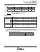
Processor frequency (signal MCLK) f
V
CC
= 1.8 V DC 4.15
MHz
Processor frequency (signal MCLK), f
(System)
V
CC
= 3.6 V DC 8
MHz
NOTES: 1. It is recommended to power AV
CC
and DV
CC
from the same source. A maximum difference of 0.3 V betweeen AV
CC
and DV
CC
can
be tolerated during power up and operation.
2. In LF mode, the LFXT1 oscillator requires a watch crystal. In XT1 mode, LFXT1 accepts a ceramic resonator or a crystal.
1.8 3.63
4.15 MHz
8 MHz
Supply Voltage − V
Supply voltage range, MSP430F42x0,
during flash memory programming
Supply voltage range,
MSP430F42x0, during
program execution
2.5
f
System
(MHz)
Figure 1. Frequency vs Supply Voltage, typical characteristic