
Datasheet


MSP430F41x2
MIXED SIGNAL MICROCONTROLLER
SLAS648E -- APRIL 2009 -- REVISED MARCH 2011
65
POST OFFICE BOX 655303 DALLAS, TEXAS 75265
APPLICATION INFORMATION
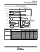
Port P6 pin schematic: P6.3 and P6.4, input/output with Schmitt trigger
P6.3/UCB0STE/
UCA0CLK/A3/CA5/
V
eref-
/V
ref-
P6.4/UCB0CLK/
UCA0STE/A4/CA6/
V
eref+
/V
ref+
Direction
0: Input
1: Output
P6SEL.x
P6DIR.x
Module Out
P6OUT.x
Pad Logic
1
0
1
0
Bus
Keeper
EN
To ADC10
ADC10AE0.3/4
INCH=3/4
CAPD.5/6
From Comparator_A
To Comparator_A
from Module
P6IN.x
D
EN
Module X IN
Port P6 (P6.3 and P6.4) pin functions
P
I
N
N
A
M
E
(
P
6
X
)
X
F
U
N
C
T
I
O
N
CONTROL BITS / SIGNALS
PIN N
A
ME (P6.
X
)
X
FUNCTION
CAPD ADC10AE0.y P6DIR.x P6SEL.x
P6.3/UCB0STE/ 3
P6.x (I/O) 0 0 I: 0, O: 1 0
/
/
UCA0CLK/A3/CA5/
/
V
f
/
V
f
UCB0STE/UCA0CLK (see Note 2) 0 0 x 1
/
V
eref--
/
V
ref--
A3/V
eref--
/V
ref--
x 1(y=3) x x
CA5 1 (CAPD.5) x x x
P6.4/UCB0CLK/ 4
P6.x (I/O) 0 0 I: 0, O: 1 0
/
/
UCA0STE/A4/CA6/
/
V
f
/
V
f
UCB0CLK/UCA0STE (see Note 2) 0 0 x 1
/
V
eref+
/
V
ref+
A4/V
eref+
/V
ref+
x 1(y=4) x x
CA6 1 (CAPD.6) x x x
NOTES: 1. x: Don’t care
2. The pin direction is controlled by the USCI module.