
Datasheet

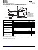


Direction
0: Input
1: Output
P6SEL.7
P6DIR.7
P6IN.7
D
EN
Module X IN
Module X OUT
P6OUT.7
P6.7/A7/SVSIN
DVSS
DVCC
P6REN.7
Pad Logic
1
1
0
1
0
1
0
Bus
Keeper
EN
ADC12 A7
VLD = 15
To SVS Mux
From ADC12
MSP430F23x
MSP430F24x(1)
MSP430F2410
www.ti.com
SLAS547I –JUNE 2007–REVISED DECEMBER 2012
Port P6 Pin Schematic: P6.7, Input/Output With Schmitt Trigger
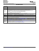
Table 28. Port P6.7 Pin Functions
CONTROL BITS / SIGNALS
(1)
PIN NAME (P6.x) x FUNCTION
P6DIR.x P6SEL.x INCHy
P6.7 (I/O) I: 0; O: 1 0 0
DV
SS
1 1 0
P6.7/A7/SVSIN 7
A7
(2)
X X 1 (y = 7)
SVSIN (VLD = 15) X X 1
(1) X = Don't care
(2) MSP430F24x and MSP430F23x devices only
Copyright © 2007–2012, Texas Instruments Incorporated Submit Documentation Feedback 77