
Datasheet


MSP430F23x
MSP430F24x(1)
MSP430F2410
www.ti.com
SLAS547I –JUNE 2007–REVISED DECEMBER 2012
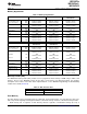
Table 3. Terminal Functions, MSP430F24x, MSP430F2410
TERMINAL
I/O DESCRIPTION
NAME NO.
AV
CC
64 Analog supply voltage, positive terminal. Supplies only the analog portion of ADC12.
AV
SS
62 Analog supply voltage, negative terminal. Supplies only the analog portion of ADC12.
DV
CC
1 Digital supply voltage, positive terminal. Supplies all digital parts.
DV
SS
63 Digital supply voltage, negative terminal. Supplies all digital parts.
P1.0/TACLK/CAOUT 12 I/O General-purpose digital I/O / Timer_A, clock signal TACLK input/Comparator_A output
P1.1/TA0 13 I/O General-purpose digital I/O / Timer_A, capture: CCI0A input, compare: Out0 output/BSL transmit
P1.2/TA1 14 I/O General-purpose digital I/O / Timer_A, capture: CCI1A input, compare: Out1 output
P1.3/TA2 15 I/O General-purpose digital I/O / Timer_A, capture: CCI2A input, compare: Out2 output
P1.4/SMCLK 16 I/O General-purpose digital I/O / SMCLK signal output
P1.5/TA0 17 I/O General-purpose digital I/O / Timer_A, compare: Out0 output
P1.6/TA1 18 I/O General-purpose digital I/O / Timer_A, compare: Out1 output
P1.7/TA2 19 I/O General-purpose digital I/O / Timer_A, compare: Out2 output
P2.0/ACLK/CA2 20 I/O General-purpose digital I/O / ACLK output/Comparator_A input
P2.1/TAINCLK/CA3 21 I/O General-purpose digital I/O / Timer_A, clock signal at INCLK
General-purpose digital I/O / Timer_A, capture: CCI0B input / Comparator_A output/BSL
P2.2/CAOUT/TA0/CA4 22 I/O
receive/Comparator_A input
P2.3/CA0/TA1 23 I/O General-purpose digital I/O / Timer_A, compare: Out1 output / Comparator_A input
P2.4/CA1/TA2 24 I/O General-purpose digital I/O / Timer_A, compare: Out2 output / Comparator_A input
General-purpose digital I/O / Input for external resistor defining the DCO nominal frequency / Comparator_A
P2.5/R
OSC
/CA5 25 I/O
input
P2.6/ADC12CLK/CA6 26 I/O General-purpose digital I/O / Conversion clock - 12-bit ADC / Comparator_A input
P2.7/TA0/CA7 27 I/O General-purpose digital I/O / Timer_A, compare: Out0 output / Comparator_A input
P3.0/UCB0STE/ UCA0CLK 28 I/O General-purpose digital I/O / USCI_B0 slave transmit enable / USCI A0 clock input/output
P3.1/UCB0SIMO/UCB0SDA 29 I/O
General-purpose digital I/O / USCI_B0 slave in/master out in SPI mode, SDA I
2
C data in I
2
C mode
P3.2/UCB0SOMI/ UCB0SCL 30 I/O
General-purpose digital I/O / USCI_B0 slave out/master in in SPI mode, SCL I
2
C clock in I
2
C mode
P3.3/UCB0CLK/UCA0STE 31 I/O General-purpose digital I/O / USCI_B0 clock input/output, USCI A0 slave transmit enable
General-purpose digital I/O / USCI_A- transmit data output in UART mode, slave data in/master out in SPI
P3.4/UCA0TXD/UCA0SIMO 32 I/O
mode
P3.5/UCA0RXD/ General-purpose digital I/O / USCI_A0 receive data input in UART mode, slave data out/master in in SPI
33 I/O
UCA0SOMI mode
General-purpose digital I/O / USCI_A1 transmit data output in UART mode, slave data in/master out in SPI
P3.6/UCA1TXD/UCA1SIMO 34 I/O
mode
P3.7/UCA1RXD/ General-purpose digital I/O / USCI_A1 receive data input in UART mode, slave data out/master in in SPI
35 I/O
UCA1SOMI mode
P4.0/TB0 36 I/O General-purpose digital I/O / Timer_B, capture: CCI0A/B input, compare: Out0 output
P4.1/TB1 37 I/O General-purpose digital I/O / Timer_B, capture: CCI1A/B input, compare: Out1 output
P4.2/TB2 38 I/O General-purpose digital I/O / Timer_B, capture: CCI2A/B input, compare: Out2 output
P4.3/TB3 39 I/O General-purpose digital I/O / Timer_B, capture: CCI3A/B input, compare: Out3 output
P4.4/TB4 40 I/O General-purpose digital I/O / Timer_B, capture: CCI4A/B input, compare: Out4 output
P4.5/TB5 41 I/O General-purpose digital I/O / Timer_B, capture: CCI5A/B input, compare: Out5 output
P4.6/TB6 42 I/O General-purpose digital I/O / Timer_B, capture: CCI6A input, compare: Out6 output
P4.7/TBCLK 43 I/O General-purpose digital I/O / Timer_B, clock signal TBCLK input
P5.0/UCB1STE/UCA1CLK 44 I/O General-purpose digital I/O / USCI_B1 slave transmit enable / USCI_A1 clock input/output
P5.1/UCB1SIMO/UCB1SDA 45 I/O
General-purpose digital I/O / USCI_B1 slave in/master out in SPI mode, SDA I
2
C data in I
2
C mode
P5.2/UCB1SOMI/UCB1SCL 46 I/O
General-purpose digital I/O / USCI_B1 slave out/master in in SPI mode, SCL I
2
C clock in I
2
C mode
P5.3/UCB1CLK/UCA1STE 47 I/O General-purpose digital I/O / USCI_B1 clock input/output, USCI_A1 slave transmit enable
P5.4/MCLK 48 I/O General-purpose digital I/O / main system clock MCLK output
P5.5/SMCLK 49 I/O General-purpose digital I/O / submain system clock SMCLK output
P5.6/ACLK 50 I/O General-purpose digital I/O / auxiliary clock ACLK output
General-purpose digital I/O / switch all PWM digital output ports to high impedance - Timer_B TB0 to
P5.7/TBOUTH/SVSOUT 51 I/O
TB6/SVS comparator output
P6.0/A0 59 I/O General-purpose digital I/O / analog input A0 - 12-bit ADC
Copyright © 2007–2012, Texas Instruments Incorporated Submit Documentation Feedback 11