
Datasheet


MSP430F23x
MSP430F24x(1)
MSP430F2410
www.ti.com
SLAS547I –JUNE 2007–REVISED DECEMBER 2012
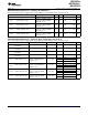
Crystal Oscillator LFXT1, High-Frequency Mode
(1)
PARAMETER TEST CONDITIONS V
CC
MIN TYP MAX UNIT
LFXT1 oscillator crystal
f
LFXT1,HF0
XTS = 1, LFXT1Sx = 0, XCAPx = 0 1.8 V to 3.6 V 0.4 1 MHz
frequency, HF mode 0
LFXT1 oscillator crystal
f
LFXT1,HF1
XTS = 1, LFXT1Sx = 1, XCAPx = 0 1.8 V to 3.6 V 1 4 MHz
frequency, HF mode 1
1.8 V to 3.6 V 2 10
LFXT1 oscillator crystal
f
LFXT1,HF2
XTS = 1, LFXT1Sx = 2, XCAPx = 0 2.2 V to 3.6 V 2 12 MHz
frequency, HF mode 2
3 V to 3.6 V 2 16
1.8 V to 3.6 V 0.4 10
LFXT1 oscillator logic-level
f
LFXT1,HF,logic
square-wave input XTS = 1, LFXT1Sx = 3, XCAPx = 0 2.2 V to 3.6 V 0.4 12 MHz
frequency, HF mode
3 V to 3.6 V 0.4 16
XTS = 1, XCAPx = 0, LFXT1Sx = 0,
2700
f
LFXT1,HF
= 1 MHz, C
L,eff
= 15 pF
Oscillation allowance for HF
XTS = 1, XCAPx = 0, LFXT1Sx = 1,
OA
HF
crystals (see Figure 23 and 800 Ω
f
LFXT1,HF
= 4 MHz, C
L,eff
= 15 pF
Figure 24)
XTS = 1, XCAPx = 0, LFXT1Sx = 2,
300
f
LFXT1,HF
= 16 MHz, C
L,eff
= 15 pF
Integrated effective load
C
L,eff
XTS = 1, XCAPx = 0
(3)
1 pF
capacitance, HF mode
(2)
XTS = 1, XCAPx = 0,
Measured at P1.4/SMCLK, 40 50 60
f
LFXT1,HF
= 10 MHz
Duty cycle, HF mode 2.2 V, 3 V %
XTS = 1, XCAPx = 0,
Measured at P1.4/SMCLK, 40 50 60
f
LFXT1,HF
= 16 MHz
f
Fault,HF
Oscillator fault frequency
(4)
XTS = 1, LFXT1Sx = 3, XCAPx = 0
(5)
2.2 V, 3 V 30 300 kHz
(1) To improve EMI on the XT2 oscillator the following guidelines should be observed:
(a) Keep the trace between the device and the crystal as short as possible.
(b) Design a good ground plane around the oscillator pins.
(c) Prevent crosstalk from other clock or data lines into oscillator pins XIN and XOUT.
(d) Avoid running PCB traces underneath or adjacent to the XIN and XOUT pins.
(e) Use assembly materials and praxis to avoid any parasitic load on the oscillator XIN and XOUT pins.
(f) If conformal coating is used, ensure that it does not induce capacitive or resistive leakage between the oscillator pins.
(g) Do not route the XOUT line to the JTAG header to support the serial programming adapter as shown in other documentation. This
signal is no longer required for the serial programming adapter.
(2) Includes parasitic bond and package capacitance (approximately 2 pF per pin). Because the PCB adds additional capacitance, it is
recommended to verify the correct load by measuring the ACLK frequency. For a correct setup, the effective load capacitance should
always match the specification of the used crystal.
(3) Requires external capacitors at both terminals. Values are specified by crystal manufacturers.
(4) Frequencies below the MIN specification set the fault flag, frequencies above the MAX specification do not set the fault flag, and
frequencies in between might set the flag.
(5) Measured with logic-level input frequency, but also applies to operation with crystals.
Copyright © 2007–2012, Texas Instruments Incorporated Submit Documentation Feedback 49