
Datasheet


0
0.5
1
1.5
2
V
CC
V
CC
1 ns 1 ns
V
CC(min)
t
pw
t
pw
− Pulse Width − µs
V
CC(min)
− V
3 V
1 10 1000
t
f
t
r
t − Pulse Width − µs
100
t
pw
3 V
t
f
= t
r
Rectangular Drop
Triangular Drop
V
CC(min)
V
CC(start)
AV
CC
V
(B_IT−)
Brownout
Region
V
(SVSstart)
V
(SVS_IT−)
Software sets VLD >0:
SVS is active
t
d(SVSR)
undefined
V
hys(SVS_IT−)
0
1
t
d(BOR)
Brownout
0
1
t
d(SVSon)
t
d(BOR)
0
1
Set POR
Brown-
out
Region
SVS Circuit is Active From VLD > to V
CC
< V(
B_IT−)
SVS out
V
hys(B_IT−)
MSP430F261x
MSP430F241x
www.ti.com
SLAS541K –JUNE 2007–REVISED NOVEMBER 2012
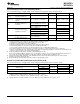
Figure 12. SVS Reset (SVSR) vs Supply Voltage
Figure 13. V
CC(min)
: Square Voltage Drop and Triangle Voltage Drop to Generate an SVS Signal (VLD = 1)
Copyright © 2007–2012, Texas Instruments Incorporated Submit Documentation Feedback 41