
Datasheet


Direction
0: Input
1: Output
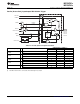
P7SEL.x
P7DIR.x
P7IN.x
D
EN
Module X IN
V
SS
P7OUT.x
P7.0
P7.1
P7.2
P7.3
P7.4
P7.5
P7.6
P7.7
DVSS
DVCC
P7REN.x
Pad Logic
1
1
0
1
0
1
0
0
MSP430F261x
MSP430F241x
SLAS541K –JUNE 2007–REVISED NOVEMBER 2012
www.ti.com
Port P7 (P7.0 to P7.7), Input/Output With Schmitt Trigger
(5)
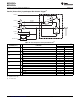
Table 24. Port P7 (P7.0 to P7.7) Pin Functions
(1)
CONTROL BITS / SIGNALS
(2)
PIN NAME (P7.x) x FUNCTION
P7DIR.x P7SEL.x
P7.0 (I/O) I: 0; O: 1 0
P7.0 0
Input X 1
P7.1 (I/O) I: 0; O: 1 0
P7.1 1
Input X 1
P7.2 (I/O) I: 0; O: 1 0
P7.2 2
Input X 1
P7.3 (I/O) I: 0; O: 1 0
P7.3 3
Input X 1
P7.4 (I/O) I: 0; O: 1 0
P7.4 4
Input X 1
P7.5 (I/O) I: 0; O: 1 0
P7.5 5
Input X 1
P7.6 (I/O) I: 0; O: 1 0
P7.6 6
Input X 1
P7.7 (I/O) I: 0; O: 1 0
P7.7 7
Input X 1
(5) 80-pin devices only
(1) 80-pin devices only
(2) X = Don't care
84 Submit Documentation Feedback Copyright © 2007–2012, Texas Instruments Incorporated