
Datasheet


MSP430F23x
MSP430F24x(1)
MSP430F2410
SLAS547I –JUNE 2007–REVISED DECEMBER 2012
www.ti.com
Digital I/O
There are up to six 8-bit I/O ports implemented—ports P1 through P6:
• All individual I/O bits are independently programmable.
• Any combination of input, output, and interrupt condition is possible.
• Edge-selectable interrupt input capability for all eight bits of port P1 and P2.
• Read/write access to port-control registers is supported by all instructions.
• Each I/O has an individually programmable pullup/pulldown resistor.
Watchdog Timer (WDT+)
The primary function of the WDT+ module is to perform a controlled system restart after a software problem
occurs. If the selected time interval expires, a system reset is generated. If the watchdog function is not needed
in an application, the module can be disabled or configured as an interval timer and can generate interrupts at
selected time intervals.
Hardware Multiplier
The multiplication operation is supported by a dedicated peripheral module. The module performs 16x16, 16x8,
8x16, and 8x8 bit operations. The module is capable of supporting signed and unsigned multiplication as well as
signed and unsigned multiply and accumulate operations. The result of an operation can be accessed
immediately after the operands have been loaded into the peripheral registers. No additional clock cycles are
required.
Timer_A3
Timer_A3 is a 16-bit timer/counter with three capture/compare registers. Timer_A3 can support multiple
capture/compares, PWM outputs, and interval timing. Timer_A3 also has extensive interrupt capabilities.
Interrupts may be generated from the counter on overflow conditions and from each of the capture/compare
registers.
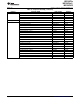
Table 16. Timer_A3 Signal Connections
DEVICE INPUT MODULE INPUT MODULE OUTPUT OUTPUT PIN
INPUT PIN NUMBER MODULE BLOCK
SIGNAL NAME SIGNAL NUMBER
12 - P1.0 TACLK TACLK
ACLK ACLK
Timer NA
SMCLK SMCLK
21 - P2.1 TAINCLK INCLK
13 - P1.1 TA0 CCI0A 13 - P1.1
22 - P2.2 TA0 CCI0B 17 - P1.5
CCR0 TA0
DV
SS
GND 27 - P2.7
DV
CC
V
CC
14 - P1.2 TA1 CCI1A 14 - P1.2
CAOUT (internal) CCI1B 18 - P1.6
CCR1 TA1
DV
SS
GND 23 - P2.3
DV
CC
V
CC
ADC12
(1)
(internal)
15 - P1.3 TA2 CCI2A 15 - P1.3
ACLK (internal) CCI2B 19 - P1.7
CCR2 TA2
DV
SS
GND 24 - P2.4
DV
CC
V
CC
(1) Not available in the MSP430F24x1 devices.
22 Submit Documentation Feedback Copyright © 2007–2012, Texas Instruments Incorporated