
Datasheet


MSP430F23x0
SLAS518E –AUGUST 2006– REVISED AUGUST 2011
www.ti.com
Hardware Multiplier
The multiplication operation is supported by a dedicated peripheral module. The module performs 16×16, 16×8,
8×16, and 8×8 bit operations. The module is capable of supporting signed and unsignedmultiplication as well as
signed and unsignedmultiply and accumulate operations. The result of an operation can be accessed
immediately after the operands have been loaded into the peripheral registers. No additional clock cycles are
required.
Comparator_A+
The primary function of the comparator_A+ module is to support precision slope analog-to-digital conversions,
battery-voltage supervision, and monitoring of external analog signals.
Timer_A3
Timer_A3 is a 16-bit timer/counter with three capture/compare registers. Timer_A3 can support multiple
capture/compares, PWM outputs, and interval timing. Timer_A3 also has extensive interrupt capabilities.
Interrupts may be generated from the counter on overflow conditions and from each of the capture/compare
registers.
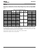
Table 14. Timer_A3 Signal Connections
INPUT PIN NUMBER MODULE OUTPUT PIN NUMBER
DEVICE INPUT MODULE MODULE
OUTPUT
SIGNAL INPUT NAME BLOCK
YFF RHA YFF RHA
SIGNAL
B4 – P1.0 4 – P1.0 TACLK TACLK
ACLK ACLK
Timer NA
SMCLK SMCLK
C7 – P2.1 13 – P2.1 TAINCLK INCLK
C4 – P1.1 5 – P1.1 TA0 CCI0A C4 – P1.1 5 – P1.1
C6 – P2.2 14 – P2.2 TA0 CCI0B B6 – P1.5 9 - P1.5
CCR0 TA0
V
SS
GND
V
CC
V
CC
A5 – P1.2 6 – P1.2 TA1 CCI1A A5 – P1.2 6 – P1.2
CAOUT
CCI1B A7 – P1.6 10 – P1.6
(internal)
CCR1 TA1
V
SS
GND D7 – P2.3 15 – P2.3
V
CC
V
CC
B5 – P1.3 7 – P1.3 TA2 CCI2A B5 – P1.3 7 – P1.3
ACLK (internal) CCI2B B7 – P1.7 11 – P1.7
CCR2 TA2
V
SS
GND D6 – P2.4 16 – P2.4
V
CC
V
CC
14 Copyright © 2006–2011, Texas Instruments Incorporated