
Datasheet


LFXT1 off
P2SEL.6
Bus
Keeper
EN
Direction
0: Input
1: Output
P2SEL.7
1
0
P2DIR.7
P2IN.7
P2IRQ.7
D
EN
Module X IN
1
0
Module X OUT
P2OUT.7
Interrupt
Edge
Select
Q
EN
Set
P2SEL.7
P2IES.7
P2IFG.7
P2IE.7
P2.7/XOUT
1
0
DVSS
DVCC
P2REN.7
Pad Logic
LFXT1 Oscillator
BCSCTL3.LFXT1Sx = 11
0
1
1
LFXT1CLK
From P2.6/XIN
P2.6/XIN
MSP430F22x2
MSP430F22x4
SLAS504G –JULY 2006–REVISED AUGUST 2012
www.ti.com
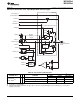
Port P2 Pin Schematic: P2.7, Input/Output With Schmitt Trigger and Crystal Oscillator Output
Table 30. Port P2 (P2.7) Pin Functions
CONTROL BITS/SIGNALS
(1)
PIN NAME (P2.x) x FUNCTION
P2DIR.x P2SEL.x
P2.7 (I/O) I: 0; O: 1 0
XOUT/P2.7 7
XOUT
(2) (3)
X 1
(1) X = Don't care
(2) Default after reset (PUC/POR)
(3) If the pin XOUT/P2.7 is used as an input a current can flow until P2SEL.7 is cleared due to the oscillator output driver connection to this
pin after reset.
68 Copyright © 2006–2012, Texas Instruments Incorporated