
Datasheet


MSP430F22x2
MSP430F22x4
SLAS504G –JULY 2006–REVISED AUGUST 2012
www.ti.com
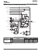
Table 26. Port P2 (P2.3) Pin Functions
CONTROL BITS/SIGNALS
(1)
PIN NAME (P2.x) x y FUNCTION
P2DIR.x P2SEL.x ADC10AE0.y
P2.3
(2)
(I/O) I: 0; O: 1 0 0
Timer_A3.CCI1B 0 1 0
P2.3/TA1/A3/V
REF-
3 3
/V
eREF-
/ OA1I1/OA1O
Timer_A3.TA1 1 1 0
A3/V
REF-
/V
eREF-
/OA1I1/OA1O
(3)
X X 1
(1) X = Don't care
(2) Default after reset (PUC/POR)
(3) Setting the ADC10AE0.y bit disables the output driver as well as the input Schmitt trigger to prevent parasitic cross currents when
applying analog signals.
64 Copyright © 2006–2012, Texas Instruments Incorporated