
Datasheet


SLAS491A − AUGUST 2005 − REVISED OCTOBER 2005
65
POST OFFICE BOX 655303 • DALLAS, TEXAS 75265
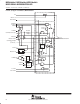
Port P2 (P2.7) pin schematics, MSP430x20x2
LFXT1 off
P2SEL.6
Bus
Keeper
EN
Direction
0: Input
1: Output
P2SEL.7
1
0
P2DIR.7
P2IN.7
P2IRQ.7
D
EN
Module X IN
1
0
Module X OUT
P2OUT.7
Interrupt
Edge
Select
Q
EN
Set
P2SEL.7
P2IES.7
P2IFG.7
P2IE.7
P2.7/XOUT
1
0
DVSS
DVCC
P2REN.7
Pad Logic
LFXT1 Oscillator
BCSCTL3.LFXT1Sx = 11
0
1
1
LFXT1CLK
From P2.6/XIN
P2.6/XIN/TA1
Port P2 (P2.7) pin functions, MSP430x20x2
PIN NAME (P2.X)
X
FUNCTION
CONTROL BITS / SIGNALS
PIN NAME (P2.X)
X
FUNCTION
P2DIR.x P2SEL.x
P2.7/XOUT
7
P2.7 Input/Output 0/1 0
P2.7/XOUT
7
DVSS 0 1
XOUT† (see Note 3) 1 1
†
Default after reset (PUC/POR)
NOTES: 1. N/A: Not available or not applicable.
2. X: Don’t care.
3. If the pin P2.7/XOUT is used as an input a current can flow until P2SEL.7 is cleared due to the oscillator output driver connection
to this pin after reset.