
Datasheet


Bus
Keeper
EN
Direction
0: Input
1: Output
P2SEL.6
1
0
P2DIR.6
P2IN.6
P2IRQ.6
D
EN
Module X IN
1
0
Module X OUT
P2OUT.6
Interrupt
Edge
Select
Q
EN
Set
P2SEL.6
P2IES.6
P2IFG.6
P2IE.6
P2.6/XIN/TA1
1
0
DVSS
DVCC
P2REN.6
Pad Logic
LFXT1 Oscillator
BCSCTL3.LFXT1Sx = 11
P2.7/XOUT
LFXT1 off
0
1
1
LFXT1CLK
P2SEL.7
MSP430F20x3
MSP430F20x2
MSP430F20x1
SLAS491I –AUGUST 2005–REVISED DECEMBER 2012
www.ti.com
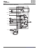
Port P2 (P2.6) Pin Schematics, MSP430F20x2
Table 26. Port P2 (P2.6) Pin Functions, MSP430F20x2
CONTROL BITS / SIGNALS
PIN NAME (P2.x) x FUNCTION
P2DIR.x P2SEL.x
P2.6 input/output 0/1 0
P2.6/XIN/TA1 6 XIN
(1)(2)
0 1
Timer_A2.TA1 1 1
(1) Default after reset (PUC/POR)
(2) XIN is used as digital clock input if the bits LFXT1Sx in register BCSCTL3 are set to 11.
64 Submit Documentation Feedback Copyright © 2005–2012, Texas Instruments Incorporated