
Datasheet


MSP430F15x, MSP430F16x, MSP430F161x
MIXED SIGNAL MICROCONTROLLER
SLAS368G − OCTOBER 2002 − REVISED MARCH 2011
47
POST OFFICE BOX 655303 • DALLAS, TEXAS 75265
electrical characteristics over recommended operating free-air temperature (unless otherwise
noted)
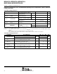
12-bit DAC, reference input specifications
PARAMETER TEST CONDITIONS V
CC
MIN TYP MAX UNIT
Ve
Reference input
DAC12IR=0 (see Notes 1 and 2) 2.2V/3V AV
CC
/3 AV
CC
+0.2
V
Ve
REF+
Reference
input
voltage range
DAC12IR=1 (see Notes 3 and 4)
2.2V/3V AVcc AVcc+0.2
V
DAC12_0 IR = DAC12_1 IR = 0 2.2V/3V 20 MΩ
DAC12_0 IR = 1, DAC12_1 IR = 0 2.2V/3V
40
48
56
kΩ
Ri
(VREF+)
,
Ri
Reference input
it
DAC12_0 IR = 0, DAC12_1 IR = 1 2.2V/3V
40 48 56 kΩ
(VREF+)
Ri
(VeREF+)
p
resistance
DAC12_0 IR = DAC12_1 IR =1,
DAC12_0 SREFx = DAC12_1 SREFx
(see Note 5)
2.2V/3V 20 24 28 kΩ
NOTES: 1. For a full-scale output, the reference input voltage can be as high as 1/3 of the maximum output voltage swing (AV
CC
).
2. The maximum voltage applied at reference input voltage terminal Ve
REF+
= [AV
CC
− V
E(O)
] / [3*(1 + E
G
)].
3. For a full-scale output, the reference input voltage can be as high as the maximum output voltage swing (AV
CC
).
4. The maximum voltage applied at reference input voltage terminal Ve
REF+
= [AV
CC
− V
E(O)
] / (1 + E
G
).
5. When DAC12IR = 1 and DAC12SREFx = 0 or 1 for both channels, the reference input resistive dividers for each DAC are in parallel
reducing the reference input resistance.
12-bit DAC, dynamic specifications; V
ref
= V
CC
, DAC12IR = 1 (see Figure 23 and Figure 24)
PARAMETER TEST CONDITIONS V
CC
MIN TYP MAX UNIT
DAC12_xDAT = 800h,
DAC12AMPx = 0 → {2, 3, 4} 2.2V/3V 60 120
t
ON
DAC12
on
-
time
_
,
Error
V(O)
< ±0.5 LSB
(see Note
DAC12AMPx = 0 → {5, 6} 2.2V/3V 15 30
μs
ON
on-
ti
me
(
see
N
o
t
e
1,Figure 23)
DAC12AMPx = 0 → 7 2.2V/3V 6 12
μ
S ttli ti
DAC12 DAT
DAC12AMPx = 2 2.2V/3V 100 200
t
S
(
FS
)
Settling time,
full
-
scale
DAC12_xDAT =
80h→ F7Fh→ 80h
DAC12AMPx = 3,5 2.2V/3V 40 80
μs
t
S(FS)
f
u
ll
-sca
l
e
80h
→
F7Fh
→
80h
DAC12AMPx = 4,6,7 2.2V/3V 15 30
μs
S ttli ti
DAC12 xDAT
=
DAC12AMPx = 2 2.2V/3V 5
t
S
(
C-C
)
Settling time,
code to code
DAC12
_
xDAT
=
3F8h→ 408h→ 3F8h
DAC12AMPx = 3,5 2.2V/3V 2
μs
t
S(C
-
C)
co
d
e
t
o co
d
e
3F8h→
408h→
3F8h
BF8h→ C08h→ BF8h
DAC12AMPx = 4,6,7 2.2V/3V 1
μs
DAC12 DAT
DAC12AMPx = 2 2.2V/3V 0.05 0.12
SR Slew rate
DAC12_xDAT =
80h→ F7Fh→ 80h
DAC12AMPx = 3,5 2.2V/3V 0.35 0.7
V/μs
SR
Slew
rate
80h
→
F7Fh
→
80h
DAC12AMPx = 4,6,7 2.2V/3V 1.5 2.7
V/μs
DAC12 DAT
DAC12AMPx = 2 2.2V/3V 10
Glitch energy: full-scale
DAC12_xDAT =
80h→ F7Fh→ 80h
DAC12AMPx = 3,5 2.2V/3V 10
nV-s
Glitch
energy:
full scale
80h
→
F7Fh
→
80h
DAC12AMPx = 4,6,7 2.2V/3V 10
nV s
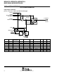
NOTES: 1. R
Load
and C
Load
connected to AV
SS
(not AV
CC
/2) in Figure 23.
2. Slew rate applies to output voltage steps ≥ 200mV.
R
Load
AV
CC
C
Load
= 100pF
2
DAC Output
R
O/P(DAC12.x)
I
Load
Conversion 1 Conversion 2
V
OUT
Conversion 3
Glitch
Energy
+/− 1/2 LSB
+/− 1/2 LSB
t
settleLH
t
settleHL
= 3 kΩ
Figure 23. Settling Time and Glitch Energy Testing