
Datasheet


MSP430F15x, MSP430F16x, MSP430F161x
MIXED SIGNAL MICROCONTROLLER
SLAS368G − OCTOBER 2002 − REVISED MARCH 2011
38
POST OFFICE BOX 655303 • DALLAS, TEXAS 75265
electrical characteristics over recommended operating free-air temperature (unless otherwise
noted) (continued)
main DCO characteristics
D Individual devices have a minimum and maximum operation frequency. The specified parameters for
f
(
DCOx0)
to f
(
DCOx7)
are valid for all devices.
D All ranges selected by Rsel(n) overlap with Rsel(n+1): Rsel0 overlaps Rsel1, ... Rsel6 overlaps Rsel7.
D DCO control bits DCO0, DCO1, and DCO2 have a step size as defined by parameter S
DCO
.
D Modulation control bits MOD0 to MOD4 select how often f
(
DCO+1)
is used within the period of 32 DCOCLK
cycles. The frequency f
(DCO)
is used for the remaining cycles. The frequency is an average equal to:
f
average
+
32 f
(DCO)
f
(DCO)1)
MOD f
(DCO)
)(32*MOD) f
(DCO)1)
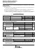
DCO when using R
OSC
(see Note 1)
PARAMETER TEST CONDITIONS V
CC
MIN TYP MAX UNIT
f DCO output frequency
R
se
l
= 4, DCO = 3, MOD = 0, DCOR = 1,
2.2 V 1.8±15% MHz
f
DCO
, DCO output frequency
R
sel
=
4
,
DCO
=
3
,
MOD
=
0
,
DCOR
=
1
,
T
A
= 25°C
3 V 1.95±15% MHz
D
t
, Temperature drift R
sel
= 4, DCO = 3, MOD = 0, DCOR = 1 2.2 V/3 V ±0.1 %/°C
D
v
, Drift with V
CC
variation R
sel
= 4, DCO = 3, MOD = 0, DCOR = 1 2.2 V/3 V 10 %/V
NOTES: 1. R
OSC
= 100kΩ. Metal film resistor, type 0257. 0.6 watt with 1% tolerance and T
K
= ±50ppm/°C.
crystal oscillator, LFXT1 oscillator (see Note 1)
PARAMETER TEST CONDITIONS MIN TYP MAX UNIT
C
Integrated input capacitance
XTS=0; LF oscillator selected, V
CC
= 2.2 V/3 V 12
pF
C
XIN
Integrated input capacitance
XTS=1; XT1 oscillator selected, V
CC
= 2.2 V/3 V 2
pF
C
Integrated output capacitance
XTS=0; LF oscillator selected, V
CC
= 2.2 V/3 V 12
pF
C
XOUT
Integrated output capacitance
XTS=1; XT1 oscillator selected, V
CC
= 2.2 V/3 V 2
pF
V
IL
I t l l t XIN
V
CC
= 2.2 V/3 V
(N2)
XTS = 0 or 1
XT1 or LF modes
V
SS
0.2 × V
CC
V
V
Input levels at XIN
CC
(see Note 2)
XTS = 0, LF mode 0.9 × V
CC
V
CC
V
V
IH
XTS = 1, XT1 mode 0.8 × V
CC
V
CC
NOTES: 1. The oscillator needs capacitors at both terminals, with values specified by the crystal manufacturer.
2. Applies only when using an external logic-level clock source. Not applicable when using a crystal or resonator.
crystal oscillator, XT2 oscillator (see Note 1)
PARAMETER TEST CONDITIONS MIN TYP MAX UNIT
C
XIN
Integrated input capacitance V
CC
= 2.2 V/3 V 2 pF
C
XOUT
Integrated output capacitance V
CC
= 2.2 V/3 V 2 pF
V
IL
Input levels at XIN
V = 2 2 V/3 V (see Note 2)
V
SS
0.2 × V
CC
V
V
IH
Input levels at XIN V
CC
= 2.2 V/3 V (see Note 2)
0.8 × V
CC
V
CC
V
NOTES: 1. The oscillator needs capacitors at both terminals, with values specified by the crystal manufacturer.
2. Applies only when using an external logic-level clock source. Not applicable when using a crystal or resonator.
USART0, USART1 (see Note 1)
PARAMETER TEST CONDITIONS MIN TYP MAX UNIT
t
( )
USART0/USART1: deglitch time
V
CC
= 2.2 V 200 430 800
ns
t
(
τ
)
USART0/USART1: deglitch time
V
CC
= 3 V 150 280 500
ns
NOTE 1: The signal applied to the USART0/USART1 receive signal/terminal (URXD0/1) should meet the timing requirements of t
(τ
)
to ensure
that the URXS flip-flop is set. The URXS flip-flop is set with negative pulses meeting the minimum-timing condition of t
(τ
)
. The operating
conditions to set the flag must be met independently from this timing constraint. The deglitch circuitry is active only on negative
transitions on the URXD0/1 line.