SLAS272F − JULY 2000 − REVISED JUNE 2004 D Low Supply-Voltage Range, 1.8 V . . . 3.6 V D Ultralow-Power Consumption: D D D D D D D D − Active Mode: 280 µA at 1 MHz, 2.2V − Standby Mode: 1.6 µA − Off Mode (RAM Retention): 0.
SLAS272F − JULY 2000 − REVISED JUNE 2004 AVAILABLE OPTIONS PACKAGED DEVICES TA PLASTIC 64-PIN QFP (PM) −40°C to 85°C MSP430F133IPM MSP430F135IPM MSP430F147IPM MSP430F1471IPM MSP430F148IPM MSP430F1481IPM MSP430F149IPM MSP430F1491IPM PLASTIC 64-PIN QFP (PAG) PLASTIC 64-PIN QFN (RTD) MSP430F133IPAG MSP430F135IPAG MSP430F147IPAG MSP430F148IPAG MSP430F149IPAG MSP430F133IRTD MSP430F135IRTD MSP430F147IRTD MSP430F1471IRTD MSP430F148IRTD MSP430F1481I
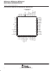
SLAS272F − JULY 2000 − REVISED JUNE 2004 pin designation, MSP430F147, MSP430F148, MSP430F149 1 64 63 62 61 60 59 58 57 56 55 54 53 52 51 50 49 48 2 47 3 46 4 45 5 44 6 43 7 42 8 41 9 40 10 39 11 38 12 37 13 36 14 35 15 34 33 16 17 18 19 20 21 22 23 24 25 26 27 28 29 30 31 32 P5.4/MCLK P5.3/UCLK1 P5.2/SOMI1 P5.1/SIMO1 P5.0/STE1 P4.7/TBCLK P4.6/TB6 P4.5/TB5 P4.4/TB4 P4.3/TB3 P4.2/TB2 P4.1/TB1 P4.0/TB0 P3.7/URXD1 P3.
SLAS272F − JULY 2000 − REVISED JUNE 2004 pin designation, MSP430F1471, MSP430F1481, MSP430F1491 1 64 63 62 61 60 59 58 57 56 55 54 53 52 51 50 49 48 2 47 3 46 4 45 5 44 6 43 7 42 8 41 9 40 10 39 11 38 12 37 13 36 14 35 15 34 33 16 17 18 19 20 21 22 23 24 25 26 27 28 29 30 31 32 P1.5/TA0 P1.6/TA1 P1.7/TA2 P2.0/ACLK P2.1/TAINCLK P2.2/CAOUT/TA0 P2.3/CA0/TA1 P2.4/CA1/TA2 P2.5/Rosc P2.6 P2.7/TA0 P3.0/STE0 P3.1/SIMO0 P3.
SLAS272F − JULY 2000 − REVISED JUNE 2004 functional block diagrams MSP430x13x XIN XOUT DVCC DVSS AVCC P1 AVSS RST/NMI P2 8 ROSC Oscillator XT2IN System Clock XT2OUT ACLK 16KB Flash 512B RAM ADC12 SMCLK 8KB Flash 256B RAM 12-Bit 8 Channels <10µs Conv.
SLAS272F − JULY 2000 − REVISED JUNE 2004 functional block diagrams (continued) MSP430x14x1 XIN XOUT DVCC DVSS AVCC P1 AVSS RST/NMI 8 ROSC Oscillator XT2IN System Clock XT2OUT ACLK 60KB Flash 2KB RAM SMCLK 48KB Flash 2KB RAM 32KB Flash 1KB RAM P2 P3 8 I/O Port 1/2 16 I/Os, with Interrupt Capability P4 8 P5 8 P6 8 I/O Port 3/4 16 I/Os 8 I/O Port 5/6 16 I/Os MCLK Test MAB, 4 Bit MAB,MAB, 16 Bit16-Bit JTAG CPU MCB E
SLAS272F − JULY 2000 − REVISED JUNE 2004 Terminal Functions MSP430x13x, MSP430x14x TERMINAL NAME NO. I/O DESCRIPTION AVCC AVSS 64 Analog supply voltage, positive terminal. Supplies the analog portion of the analog-to-digital converter. 62 Analog supply voltage, negative terminal. Supplies the analog portion of the analog-to-digital converter. DVCC 1 Digital supply voltage, positive terminal. Supplies all digital parts.
SLAS272F − JULY 2000 − REVISED JUNE 2004 Terminal Functions (Continued) MSP430x13x, MSP430x14x (continued) TERMINAL NAME NO. I/O DESCRIPTION P5.6/ACLK 50 I/O General-purpose digital I/O pin/auxiliary clock ACLK output P5.7/TBOUTH 51 I/O General-purpose digital I/O pin/switch all PWM digital output ports to high impedance − Timer_B7: TB0 to TB6 P6.0/A0 59 I/O General-purpose digital I/O pin/analog input a0 – 12-bit ADC P6.
SLAS272F − JULY 2000 − REVISED JUNE 2004 Terminal Functions MSP430x14x1 TERMINAL NAME NO. I/O DESCRIPTION AVCC AVSS 64 Analog supply voltage, positive terminal. 62 Analog supply voltage, negative terminal. DVCC 1 Digital supply voltage, positive terminal. Supplies all digital parts. DVSS 63 Digital supply voltage, negative terminal. Supplies all digital parts. P1.
SLAS272F − JULY 2000 − REVISED JUNE 2004 Terminal Functions (Continued) MSP430x14x1 (continued) TERMINAL NAME NO. I/O DESCRIPTION P5.6/ACLK 50 I/O General-purpose digital I/O pin/auxiliary clock ACLK output P5.7/TBOUTH 51 I/O General-purpose digital I/O pin/switch all PWM digital output ports to high impedance − Timer_B7: TB0 to TB6 P6.0 59 I/O General-purpose digital I/O pin P6.1 60 I/O General-purpose digital I/O pin P6.
SLAS272F − JULY 2000 − REVISED JUNE 2004 short-form description CPU The MSP430 CPU has a 16-bit RISC architecture that is highly transparent to the application. All operations, other than program-flow instructions, are performed as register operations in conjunction with seven addressing modes for source operand and four addressing modes for destination operand.
SLAS272F − JULY 2000 − REVISED JUNE 2004 operating modes The MSP430 has one active mode and five software selectable low-power modes of operation. An interrupt event can wake up the device from any of the five low-power modes, service the request and restore back to the low-power mode on return from the interrupt program.
SLAS272F − JULY 2000 − REVISED JUNE 2004 interrupt vector addresses The interrupt vectors and the power-up starting address are located in the address range 0FFFFh − 0FFE0h. The vector contains the 16-bit address of the appropriate interrupt-handler instruction sequence.
SLAS272F − JULY 2000 − REVISED JUNE 2004 special function registers Most interrupt and module-enable bits are collected in the lowest address space. Special-function register bits not allocated to a functional purpose are not physically present in the device. This arrangement provides simple software access.
SLAS272F − JULY 2000 − REVISED JUNE 2004 module enable registers 1 and 2 7 UTXE0 Address 04h rw-0 6 URXE0 USPIE0 5 4 3 2 1 rw-0 URXE0: USART0: UART receive enable UTXE0: USART0: UART transmit enable USPIE0: USART0: SPI (synchronous peripheral interface) transmit and receive enable Address 0 7 6 05h 5 UTXE1 rw-0 4 URXE1 USPIE1 3 2 1 0 rw-0 URXE1: USART1: UART receive enable UTXE1: USART1: UART transmit enable USPIE1:
SLAS272F − JULY 2000 − REVISED JUNE 2004 flash memory The flash memory can be programmed via the JTAG port, the bootstrap loader, or in-system by the CPU. The CPU can perform single-byte and single-word writes to the flash memory. Features of the flash memory include: D Flash memory has n segments of main memory and two segments of information memory (A and B) of 128 bytes each. Each segment in main memory is 512 bytes in size.
SLAS272F − JULY 2000 − REVISED JUNE 2004 peripherals Peripherals are connected to the CPU through data, address, and control busses and can be handled using all instructions. For complete module descriptions, see the MSP430x1xx Family User’s Guide, literature number SLAU049. digital I/O There are six 8-bit I/O ports implemented—ports P1 through P6: D D D D All individual I/O bits are independently programmable.
SLAS272F − JULY 2000 − REVISED JUNE 2004 comparator_A The primary function of the comparator_A module is to support precision slope analog−to−digital conversions, battery−voltage supervision, and monitoring of external analog signals. ADC12 (Not implemented in the MSP430x14x1) The ADC12 module supports fast, 12-bit analog-to-digital conversions.
SLAS272F − JULY 2000 − REVISED JUNE 2004 timer_B7 (MSP430x14x and MSP430x14x1 Only) Timer_B7 is a 16-bit timer/counter with seven capture/compare registers. Timer_B7 can support multiple capture/compares, PWM outputs, and interval timing. Timer_B7 also has extensive interrupt capabilities. Interrupts may be generated from the counter on overflow conditions and from each of the capture/compare registers.
SLAS272F − JULY 2000 − REVISED JUNE 2004 peripheral file map PERIPHERALS WITH WORD ACCESS Watchdog Watchdog Timer control WDTCTL 0120h Timer_B7/ Timer_B3 (see Note 1) Timer_B interrupt vector TBIV 011Eh Timer_B control TBCTL 0180h Capture/compare control 0 TBCCTL0 0182h Capture/compare control 1 TBCCTL1 0184h Capture/compare control 2 TBCCTL2 0186h Capture/compare control 3 TBCCTL3 0188h Capture/compare control 4 TBCCTL4 01
SLAS272F − JULY 2000 − REVISED JUNE 2004 peripheral file map (continued) PERIPHERALS WITH WORD ACCESS (CONTINUED) Flash Flash control 3 FCTL3 012Ch Flash control 2 FCTL2 012Ah Flash control 1 FCTL1 0128h ADC12 Conversion memory 15 (Not implemented in Conversion memory 14 the MSP430x14x1) Conversion memory 13 ADC12MEM15 015Eh ADC12MEM14 015Ch ADC12MEM13 015Ah Conversion memory 12 ADC12MEM12 0158h Conversion memory 11 ADC12MEM11
SLAS272F − JULY 2000 − REVISED JUNE 2004 peripheral file map (continued) PERIPHERALS WITH BYTE ACCESS USART1 (MSP430x14x and MSP430x14x1 only) USART0 Comparator_A Basic Clock Port P6 Port P5 Port P4 Port P3 Port P2 22 Transmit buffer U1TXBUF 07Fh Receive buffer U1RXBUF 07Eh Baud rate U1BR1 07Dh Baud rate U1BR0 07Ch Modulation control U1MCTL 07Bh Receive control U1RCTL 07Ah Transmit control U1TCTL 079h USART control U
SLAS272F − JULY 2000 − REVISED JUNE 2004 peripheral file map (continued) PERIPHERALS WITH BYTE ACCESS (CONTINUED) Port P1 Special Functions Port P1 selection P1SEL 026h Port P1 interrupt enable P1IE 025h Port P1 interrupt-edge select P1IES 024h Port P1 interrupt flag P1IFG 023h Port P1 direction P1DIR 022h Port P1 output P1OUT 021h Port P1 input P1IN 020h SFR module enable 2 ME2 005h SFR module enable 1 ME1 004h SFR int
SLAS272F − JULY 2000 − REVISED JUNE 2004 recommended operating conditions PARAMETER MIN NOM MAX UNITS Supply voltage during program execution, VCC (AVCC = DVCC = VCC) MSP430F13x, MSP430F14x(1) 1.8 3.6 V Supply voltage during flash memory programming, VCC (AVCC = DVCC = VCC) MSP430F13x, MSP430F14x(1) 2.7 3.6 V 0.0 0.0 V −40 85 °C 450 8000 kHz 1000 8000 kHz 450 8000 1000 8000 DC 4.
SLAS272F − JULY 2000 − REVISED JUNE 2004 electrical characteristics over recommended operating free-air temperature (unless otherwise noted) supply current into AVCC + DVCC excluding external current PARAMETER TEST CONDITIONS NOM MAX VCC = 2.2 V 280 350 VCC = 3 V 420 560 VCC = 2.2 V 2.5 7 9 20 VCC = 2.2 V VCC = 3 V 32 45 55 70 VCC = 2.2 V 11 14 VCC = 3 V 17 22 0.8 1.5 0.9 1.5 TA = 85°C TA = −40°C 1.6 2.8 1.8 2.
SLAS272F − JULY 2000 − REVISED JUNE 2004 electrical characteristics over recommended operating free-air temperature (unless otherwise noted) (continued) SCHMITT-trigger inputs − Ports P1, P2, P3, P4, P5, and P6 PARAMETER TEST CONDITIONS VIT+ Positive-going input threshold voltage VIT− Negative-going input threshold voltage Vhys Input voltage hysteresis (VIT+ − VIT−) MIN TYP MAX VCC = 2.2 V VCC = 3 V VCC = 2.2 V 1.1 1.5 1.5 1.9 0.
SLAS272F − JULY 2000 − REVISED JUNE 2004 electrical characteristics over recommended operating free-air temperature (unless otherwise noted) (continued) outputs − Ports P1, P2, P3, P4, P5, and P6 PARAMETER VOH VOL High-level output voltage Low-level output voltage TEST CONDITIONS MIN IOH(max) = −1 mA, IOH(max) = −6 mA, VCC = 2.2 V, VCC = 2.
SLAS272F − JULY 2000 − REVISED JUNE 2004 electrical characteristics over recommended operating free-air temperature (unless otherwise noted) (continued) outputs − Ports P1, P2, P3, P4, P5, and P6 (continued) TYPICAL LOW-LEVEL OUTPUT CURRENT vs LOW-LEVEL OUTPUT VOLTAGE TYPICAL LOW-LEVEL OUTPUT CURRENT vs LOW-LEVEL OUTPUT VOLTAGE 25 TA = 25°C VCC = 2.2 V P2.
SLAS272F − JULY 2000 − REVISED JUNE 2004 electrical characteristics over recommended operating free-air temperature (unless otherwise noted) (continued) wake-up LPM3 PARAMETER TEST CONDITIONS MIN TYP f = 1 MHz t(LPM3) f = 2 MHz Delay time MAX UNIT 6 6 VCC = 2.2 V/3 V f = 3 MHz µs 6 RAM PARAMETER TEST CONDITIONS VRAMh CPU HALTED (see Note 1) MIN TYP MAX 1.
SLAS272F − JULY 2000 − REVISED JUNE 2004 electrical characteristics over recommended operating free-air temperature (unless otherwise noted) (continued) 650 650 VCC = 2.
SLAS272F − JULY 2000 − REVISED JUNE 2004 electrical characteristics over recommended operating free-air temperature (unless otherwise noted) (continued) PUC/POR PARAMETER TEST CONDITIONS t(POR_Delay) Internal time delay to release POR VPOR VCC threshold at which POR release delay time begins (see Note 1) TA = −40°C TA = 25°C VCC threshold required to generate a POR (see Note 2) VCC |dV/dt| ≥ 1V/ms V(min) MIN VCC = 2.
SLAS272F − JULY 2000 − REVISED JUNE 2004 electrical characteristics over recommended operating free-air temperature (unless otherwise noted) (continued) DCO (see Note 1) PARAMETER f(DCO03) f(DCO13) f(DCO23) f(DCO33) f(DCO43) f(DCO53) f(DCO63) f(DCO73) TEST CONDITIONS MIN Rsel = 0, DCO = 3, MOD = 0, DCOR = 0, TA = 25°C Rsel = 1, DCO = 3, MOD = 0, DCOR = 0, TA = 25°C Rsel = 2, DCO = 3, MOD = 0, DCOR = 0, TA = 25°C Rsel = 3, DCO = 3, MOD = 0, DCOR
SLAS272F − JULY 2000 − REVISED JUNE 2004 electrical characteristics over recommended operating free-air temperature (unless otherwise noted) (continued) main DCO characteristics D Individual devices have a minimum and maximum operation frequency. The specified parameters for fDCOx0 to fDCOx7 are valid for all devices. D All ranges selected by Rsel(n) overlap with Rsel(n+1): Rsel0 overlaps with Rsel1, ... Rsel6 overlaps with Rsel7.
SLAS272F − JULY 2000 − REVISED JUNE 2004 electrical characteristics over recommended operating free-air temperature (unless otherwise noted) (continued) 12-bit ADC, power supply and input range conditions (see Note 1) PARAMETER TEST CONDITIONS MIN AVCC Analog supply voltage AVCC and DVCC are connected together AVSS and DVSS are connected together V(AVSS) = V(DVSS) = 0 V V(P6.x/Ax) Analog input voltage range (see Note 2) All P6.0/A0 to P6.
SLAS272F − JULY 2000 − REVISED JUNE 2004 electrical characteristics over recommended operating free-air temperature (unless otherwise noted) (continued) 12-bit ADC, built-in reference PARAMETER Positive built-in reference voltage output VREF+ AVCC(min) AVCC minimum voltage, Positive built-in reference active IVREF+ Load current out of VREF+ terminal Load-current regulation VREF+ terminal IL(VREF)+ † TEST CONDITIONS REF2_5V = 1 for 2.
SLAS272F − JULY 2000 − REVISED JUNE 2004 DVCC From Power Supply + − 10 µ F DVSS 100 nF AVCC + − 10 µ F Apply External Reference [VeREF+] or Use Internal Reference [VREF+] AVSS 10 µ F VREF+ or VeREF+ 100 nF VREF−/VeREF− + − 10 µ F MSP430F14x 100 nF + − Apply External Reference MSP430F13x 100 nF Figure 14.
SLAS272F − JULY 2000 − REVISED JUNE 2004 electrical characteristics over recommended operating free-air temperature (unless otherwise noted) (continued) 12-bit ADC, timing parameters PARAMETER TEST CONDITIONS fADC12CLK fADC12OSC Internal ADC12 oscillator MIN NOM 5 MAX UNIT 6.3 MHz For specified performance of ADC12 linearity parameters 2.2V/ 3V 0.45 ADC12DIV=0, fADC12CLK=fADC12OSC 2.2 V/ 3V 3.7 6.
SLAS272F − JULY 2000 − REVISED JUNE 2004 electrical characteristics over recommended operating free-air temperature (unless otherwise noted) (continued) 12-bit ADC, temperature sensor and built-in VMID PARAMETER TEST CONDITIONS MIN NOM MAX REFON = 0, INCH = 0Ah, ADC12ON=NA, TA = 25_C 2.2 V 40 120 3V 60 160 VSENSOR† ADC12ON = 1, INCH = 0Ah, TA = 0°C 2.2 V 986 986±5% 3V 986 986±5% TCSENSOR† 2.2 V 3.55 3.
SLAS272F − JULY 2000 − REVISED JUNE 2004 electrical characteristics over recommended operating free-air temperature (unless otherwise noted) (continued) Flash Memory TEST CONDITIONS PARAMETER VCC(PGM/ ERASE) VCC MIN NOM MAX UNIT Program and Erase supply voltage 2.7 3.6 V fFTG IPGM Flash Timing Generator frequency 257 476 kHz Supply current from DVCC during program 2.7 V/ 3.
SLAS272F − JULY 2000 − REVISED JUNE 2004 APPLICATION INFORMATION input/output schematic port P1, P1.0 to P1.7, input/output with Schmitt-trigger P1SEL.x 0 P1DIR.x Direction Control From Module 1 Pad Logic P1.0/TACLK .. 0 P1OUT.x Module X OUT 1 P1.7/TA2 P1IN.x EN Module X IN D P1IRQ.x P1IE.x Q P1IFG.x EN Set Interrupt Flag Interrupt Edge Select P1IES.x P1SEL.x PnSel.x PnDIR.x Dir. CONTROL FROM MODULE PnOUT.x MODULE X OUT PnIN.
SLAS272F − JULY 2000 − REVISED JUNE 2004 APPLICATION INFORMATION input/output schematic (continued) port P2, P2.0 to P2.2, P2.6, and P2.7 input/output with Schmitt-trigger P2SEL.x 0 P2DIR.x Direction Control From Module 0: Input 1: Output 1 0 P2OUT.x Module X OUT 1 P2.0/ACLK P2.1/TAINCLK P2.2/CAOUT/TA0 Pad Logic P2.6/ADC12CLK P2.7/TA0 P2IN.x EN Module X IN P2IRQ.x Bus Keeper D P2IE.x P2IFG.x Set Interrupt Flag CAPD.
SLAS272F − JULY 2000 − REVISED JUNE 2004 APPLICATION INFORMATION input/output schematic (continued) port P2, P2.3 to P2.4, input/output with Schmitt-trigger P2SEL.3 0: Input 1: Output 0 P2DIR.3 Direction Control From Module 1 Pad Logic P2.3/CA0/TA1 0 P2OUT.3 Module X OUT 1 P2IN.3 EN Module X IN Bus Keeper D P2IRQ.3 P2IE.3 P2IFG.3 EN Set Q Interrupt Flag Interrupt Edge Select CAPD.3 Comparator_A CAEX P2CA P2IES.3 P2SEL.
SLAS272F − JULY 2000 − REVISED JUNE 2004 APPLICATION INFORMATION input/output schematic (continued) port P2, P2.5, input/output with Schmitt-trigger and Rosc function for the basic clock module 0: Input 1: Output P2SEL.5 0 P2DIR.5 Direction Control From Module Pad Logic 1 P2.5/Rosc 0 P2OUT.5 Module X OUT 1 Bus Keeper P2IN.5 EN Module X IN P2IRQ.5 D P2IE.5 Q P2IFG.
SLAS272F − JULY 2000 − REVISED JUNE 2004 APPLICATION INFORMATION input/output schematic (continued) port P3, P3.0 and P3.4 to P3.7, input/output with Schmitt-trigger P3SEL.x 0: Input 1: Output 0 P3DIR.x Direction Control From Module 1 Pad Logic P3OUT.x Module X OUT 0 P3.0/STE0 1 P3.4/UTXD0 P3.5/URXD0 P3.6/UTXD1‡ P3.7/URXD1¶ P3IN.x EN D Module X IN x: Bit Identifier, 0 and 4 to 7 for Port P3 PnSel.x PnDIR.x P3Sel.0 P3DIR.0 P3Sel.
SLAS272F − JULY 2000 − REVISED JUNE 2004 APPLICATION INFORMATION input/output schematic (continued) port P3, P3.1, input/output with Schmitt-trigger P3SEL.1 SYNC MM STC STE 0 P3DIR.1 0: Input 1: Output 1 DCM_SIMO Pad Logic P3.1/SIMO0 0 P3OUT1 (SI)MO0 From USART0 1 P3IN.1 EN SI(MO)0 To USART0 D port P3, P3.2, input/output with Schmitt-trigger P3SEL.2 SYNC MM STC STE 0 P3DIR.2 0: Input 1: Output 1 DCM_SOMI Pad Logic P3.
SLAS272F − JULY 2000 − REVISED JUNE 2004 APPLICATION INFORMATION input/output schematic (continued) port P3, P3.3, input/output with Schmitt-trigger P3SEL.3 SYNC MM STC STE 0 P3DIR.3 0: Input 1: Output 1 DCM_UCLK Pad Logic P3.3/UCLK0 0 P3OUT.3 UCLK.0 From USART0 1 P3IN.3 EN UCLK0 D To USART0 NOTE: UART mode: The UART clock can only be an input. If UART mode and UART function are selected, the P3.3/UCLK0 is always an input.
SLAS272F − JULY 2000 − REVISED JUNE 2004 APPLICATION INFORMATION input/output schematic (continued) port P4, P4.0 to P4.6, input/output with Schmitt-trigger P4SEL.x 0 P4DIR.x Direction Control From Module Module X IN 0: Input 1: Output 1 w Pad Logic P5SEL.7 P4OUT.x Module X OUT 0 P4.0/TB0 .. 1 P4.6/TB6 TBOUTHiZ Bus Keeper P4IN.x EN Module X IN D x: bit identifier, 0 to 6 for Port P4 PnSel.x PnDIR.
SLAS272F − JULY 2000 − REVISED JUNE 2004 APPLICATION INFORMATION input/output schematic (continued) port P4, P4.7, input/output with Schmitt-trigger P4SEL.7 0: Input 1: Output 0 P4DIR.7 1 Pad Logic P4.7/TBCLK 0 P4OUT.7 DVSS 1 P4IN.7 EN Timer_B, D TBCLK port P5, P5.0 and P5.4 to P5.7, input/output with Schmitt-trigger P5SEL.x 0: Input 1: Output 0 P5DIR.x Direction Control From Module 1 Pad Logic P5OUT.x Module X OUT 0 P5.
SLAS272F − JULY 2000 − REVISED JUNE 2004 APPLICATION INFORMATION input/output schematic (continued) port P5, P5.1, input/output with Schmitt-trigger P5SEL.1 SYNC MM 0 P5DIR.1 1 DCM_SIMO STC STE 0: Input 1: Output Pad Logic P5.1/SIMO1 0 P5OUT.1 (SI)MO1 From USART1 1 P5IN.1 EN SI(MO)1 To USART1 D port P5, P5.2, input/output with Schmitt-trigger P5SEL.2 SYNC MM STC STE 0 P5DIR.2 0: Input 1: Output 1 DCM_SOMI Pad Logic P5.
SLAS272F − JULY 2000 − REVISED JUNE 2004 APPLICATION INFORMATION input/output schematic (continued) port P5, P5.3, input/output with Schmitt-trigger P5SEL.3 SYNC MM STC STE 0 P5DIR.3 0: Input 1: Output 1 DCM_SIMO Pad Logic P5.3/UCLK1 0 P5OUT.3 UCLK1 From USART1 1 P5IN.3 EN D UCLK1 To USART1 NOTE: UART mode: The UART clock can only be an input. If UART mode and UART function are selected, the P5.3/UCLK1 direction is always input.
SLAS272F − JULY 2000 − REVISED JUNE 2004 APPLICATION INFORMATION input/output schematic (continued) port P6, P6.0 to P6.7, input/output with Schmitt-trigger P6SEL.x 0 P6DIR.x Direction Control From Module 0: Input 1: Output 1 Pad Logic P6.0 .. P6.7 0 P6OUT.x Module X OUT 1 Bus Keeper P6IN.
SLAS272F − JULY 2000 − REVISED JUNE 2004 APPLICATION INFORMATION JTAG pins TMS, TCK, TDI/TCLK, TDO/TDI, input/output with Schmitt-trigger TDO Controlled by JTAG Controlled by JTAG JTAG TDO/TDI Controlled by JTAG DVCC DVCC TDI Fuse Burn & Test Fuse Test TDI/TCLK & Emulation Module DVCC TMS TMS DVCC During Programming Activity and During Blowing of the Fuse, Pin TDO/TDI Is Used to Apply the Test Input Data for JTAG Circuitry TCK TCK 52 POS
SLAS272F − JULY 2000 − REVISED JUNE 2004 APPLICATION INFORMATION JTAG fuse check mode MSP430 devices that have the fuse on the TDI/TCLK terminal have a fuse check mode that tests the continuity of the fuse the first time the JTAG port is accessed after a power-on reset (POR). When activated, a fuse check current, ITF , of 1 mA at 3 V, 2.5 mA at 5 V can flow from the TDI/TCLK pin to ground if the fuse is not burned.
PACKAGE OPTION ADDENDUM www.ti.
PACKAGE OPTION ADDENDUM www.ti.
PACKAGE OPTION ADDENDUM www.ti.
PACKAGE OPTION ADDENDUM www.ti.com 23-Nov-2013 (2) Eco Plan - The planned eco-friendly classification: Pb-Free (RoHS), Pb-Free (RoHS Exempt), or Green (RoHS & no Sb/Br) - please check http://www.ti.com/productcontent for the latest availability information and additional product content details. TBD: The Pb-Free/Green conversion plan has not been defined.
PACKAGE MATERIALS INFORMATION www.ti.com 12-Oct-2013 TAPE AND REEL INFORMATION *All dimensions are nominal Device Package Package Pins Type Drawing SPQ Reel Reel A0 Diameter Width (mm) (mm) W1 (mm) B0 (mm) K0 (mm) P1 (mm) W Pin1 (mm) Quadrant MSP430F133IPMR LQFP PM 64 1000 330.0 24.4 13.0 13.0 2.1 16.0 24.0 Q2 MSP430F135IPMR LQFP PM 64 1000 330.0 24.4 13.0 13.0 2.1 16.0 24.0 Q2 MSP430F1471IPMR LQFP PM 64 1000 330.0 24.4 13.0 13.0 2.1 16.0 24.
PACKAGE MATERIALS INFORMATION www.ti.com 12-Oct-2013 *All dimensions are nominal Device Package Type Package Drawing Pins SPQ Length (mm) Width (mm) Height (mm) MSP430F133IPMR LQFP PM 64 1000 336.6 336.6 41.3 MSP430F135IPMR LQFP PM 64 1000 336.6 336.6 41.3 MSP430F1471IPMR LQFP PM 64 1000 336.6 336.6 41.3 MSP430F147IPMR LQFP PM 64 1000 336.6 336.6 41.3 MSP430F1481IPMR LQFP PM 64 1000 336.6 336.6 41.3 MSP430F148IPMR LQFP PM 64 1000 336.6 336.6 41.
MECHANICAL DATA MTQF006A – JANUARY 1995 – REVISED DECEMBER 1996 PAG (S-PQFP-G64) PLASTIC QUAD FLATPACK 0,27 0,17 0,50 48 0,08 M 33 49 32 64 17 0,13 NOM 1 16 7,50 TYP Gage Plane 10,20 SQ 9,80 12,20 SQ 11,80 0,25 0,05 MIN 1,05 0,95 0°– 7° 0,75 0,45 Seating Plane 0,08 1,20 MAX 4040282 / C 11/96 NOTES: A. All linear dimensions are in millimeters. B. This drawing is subject to change without notice. C.
MECHANICAL DATA MTQF008A – JANUARY 1995 – REVISED DECEMBER 1996 PM (S-PQFP-G64) PLASTIC QUAD FLATPACK 0,27 0,17 0,50 0,08 M 33 48 49 32 64 17 0,13 NOM 1 16 7,50 TYP Gage Plane 10,20 SQ 9,80 12,20 SQ 11,80 0,25 0,05 MIN 0°– 7° 0,75 0,45 1,45 1,35 Seating Plane 0,08 1,60 MAX 4040152 / C 11/96 NOTES: A. B. C. D. All linear dimensions are in millimeters. This drawing is subject to change without notice.
IMPORTANT NOTICE Texas Instruments Incorporated and its subsidiaries (TI) reserve the right to make corrections, enhancements, improvements and other changes to its semiconductor products and services per JESD46, latest issue, and to discontinue any product or service per JESD48, latest issue. Buyers should obtain the latest relevant information before placing orders and should verify that such information is current and complete.